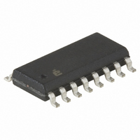
HI3338KIBZ Intersil, HI3338KIBZ Datasheet - Page 5

HI3338KIBZ
Manufacturer Part Number
HI3338KIBZ
Description
IC DAC 8BIT CMOS 16-SOIC
Manufacturer
Intersil
Datasheet
1.HI3338KIBZ.pdf
(9 pages)
Specifications of HI3338KIBZ
Settling Time
20ns
Number Of Bits
8
Data Interface
Parallel
Number Of Converters
1
Voltage Supply Source
Single Supply
Power Dissipation (max)
100mW
Operating Temperature
-40°C ~ 85°C
Mounting Type
Surface Mount
Package / Case
16-SOIC (0.300", 7.5mm Width)
Lead Free Status / RoHS Status
Lead free / RoHS Compliant
Pin Descriptions
Digital Signal Path
The digital inputs (LE, COMP, and D0 - D7) are of TTL
compatible HCT High Speed CMOS design: the loading is
essentially capacitive and the logic threshold is typically
1.5V.
The 8 data bits, D0 (weighted 2
are applied to Exclusive OR gates (see Functional Diagram).
The COMP (data complement) control provides the second
input to the gates: if COMP is high, the data bits will be
inverted as they pass through.
The input data and the LE (latch enable) signals are next
applied to a level shifter. The inputs, operating between the
levels of V
and V
will be discussed under bipolar operation. All further logic
elements except the output drivers operate from the V
and V
The upper 3 bits of data, D5 through D7, are input to a 3-to-7
line bar graph encoder. The encoder outputs and D0 through
D4 are applied to a feedthrough latch, which is controlled by
LE (latch enable).
PIN
10
11
12
13
14
15
16
1
2
3
4
5
6
7
8
9
EE
EE
. V
supplies.
DD
V
COMP Data Complement Control input. Active High
NAME
V
V
EE
V
V
V
REF
REF
D7
D6
D5
D4
D3
D2
D1
D0
OUT
LE
SS
EE
DD
and V
optionally at ground or at a negative voltage,
+ Reference Voltage Positive Input
-
Most Significant Bit
Digital Ground
Least Significant Bit. Input Data Bit
Analog Ground
Reference Voltage Negative Input
Analog Output
Latch Enable Input. Active Low
Digital Power Supply, +5V
SS
Input
Data
Bits
(High = True)
, are shifted to operate between V
5
0
DESCRIPTION
) through D7 (weighted 2
DD
DD
7
),
HI3338
Latch Operation
Data is fed from input to output while LE is low: LE should be
tied low for non-clocked operation.
Non-clocked operation or changing data while LE is low is
not recommended for applications requiring low output
“glitch” energy: there is no guarantee of the simultaneous
changing of input data or the equal propagation delay of all
bits through the converter. Several parameters are given if
the converter is to be used in either of these modes: t
gives the delay from the input changing to the output
changing (10%), while t
times (referred to LE rising edge) needed to latch data. See
Figures 1 and 2.
Clocked operation is needed for low “glitch” energy use. Data
must meet the given t
and the t
the output changing, t
edge.
There is no need for a square wave LE clock; LE must only
meet the minimum t
operation. Generally, output timing (desired accuracy of
settling) sets the upper limit of usable clock frequency.
Output Structure
The latches feed data to a row of high current CMOS drivers,
which in turn feed a modified R2R ladder network.
The “N” channel (pull down) transistor of each driver plus
the bottom “2R” resistor are returned to V
(-) full-scale reference. The “P” channel (pull up) transistor
of each driver is returned to V
reference.
In unipolar operation, V
analog ground, but may be raised above ground (see
specifications). There is substantial code dependent current
that flows from V
specifications), so V
to ground.
In bipolar operation, V
voltage (the maximum voltage rating to V
observed). V
output drivers, must be returned to a point at least as
negative as V
decreases when the bipolar mode is used.
Static Characteristics
The ideal 8-bit D/A would have an output equal to V
with an input code of 00
output equal to 255/256 of V
an input code of FF HEX (full scale output). The difference
between the ideal and actual values of these two parameters
are the OFFSET and GAIN errors, respectively; see
Figure 3.
H
hold time from the LE rising edge. The delay to
EE
REF
, which supplies the gate potential for the
REF
-. Note that the maximum clocking speed
W
REF
+ to V
SU1
D1
REF
pulse width for successful latch
REF
SU2
HEX
- should have a low impedance path
, is now referred to the LE falling
set up time to the LE falling edge,
- would be returned to a negative
REF
- would typically be returned to
and t
REF
(zero scale output), and an
REF
- (see V
+ (referred to V
H
+, the (+) full-scale
give the set up and hold
REF
DD
REF
+ input current in
must be
- this is the
REF
REF
-) with
D2
-


