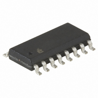
HI3338KIBZ Intersil, HI3338KIBZ Datasheet - Page 6

HI3338KIBZ
Manufacturer Part Number
HI3338KIBZ
Description
IC DAC 8BIT CMOS 16-SOIC
Manufacturer
Intersil
Datasheet
1.HI3338KIBZ.pdf
(9 pages)
Specifications of HI3338KIBZ
Settling Time
20ns
Number Of Bits
8
Data Interface
Parallel
Number Of Converters
1
Voltage Supply Source
Single Supply
Power Dissipation (max)
100mW
Operating Temperature
-40°C ~ 85°C
Mounting Type
Surface Mount
Package / Case
16-SOIC (0.300", 7.5mm Width)
Lead Free Status / RoHS Status
Lead free / RoHS Compliant
If the code into an 8-bit D/A is changed by 1 count, the
output should change by 1/255 (full-scale output-zero scale
output). A deviation from this step size is a differential
linearity error, see Figure 4. Note that the error is expressed
in fractions of the ideal step size (usually called an LSB).
Also note that if the (-) differential linearity error is less (in
absolute numbers) than 1 LSB, the device is monotonic.
(The output will always increase for increasing code or
decrease for decreasing code).
If the code into an 8-bit D/A is at any value, say “N”, the
output voltage should be N/255 of the full-scale output
(referred to the zero-scale output). Any deviation from that
output is an integral linearity error, usually expressed in
LSBs. See Figure 4.
Note that OFFSET and GAIN errors do not affect integral
linearity, as the linearity is referenced to actual zero and full
scale outputs, not ideal. Absolute accuracy would have to
also take these errors into account.
0
00
FIGURE 4. D/A INTEGRAL AND DIFFERENTIAL LINEARITY
255/256
254/256
253/256
3/256
2/256
1/256
= IDEAL TRANSFER CURVE
= ACTUAL TRANSFER CURVE
FIGURE 3. D/A OFFSET AND GAIN ERROR
0
A
00
(SHOWN +)
INPUT CODE IN HEXADECIMAL (COMP = LOW)
OFFSET
ERROR
C
01
= IDEAL TRANSFER CURVE
= ACTUAL TRANSFER CURVE
A = IDEAL STEP SIZE (1/255 OF FULL
B - A = +DIFFERENTIAL LINEARITY ERROR
C - A = -DIFFERENTIAL LINEARITY ERROR
02
B
INPUT CODE
SCALE -“0” SCALE VOLTAGE)
STRAIGHT LINE
FROM “0” SCALE
TO FULL SCALE
VOLTAGE
03
6
GAIN ERROR (SHOWN -)
INTEGRAL LINEARITY
ERROR (SHOWN -)
FD
FE
FF
HI3338
Dynamic Characteristics
Keeping the full-scale range (V
possible gives the best linearity and lowest “glitch” energy
(referred to 1V). This provides the best “P” and “N” channel
gate drives (hence saturation resistance) and propagation
delays. The V
well bypassed as near the chip as possible.
“Glitch” energy is defined as a spurious voltage that occurs
as the output is changed from one voltage to another. In a
binary input converter, it is usually highest at the most
significant bit transition (7F
and can be measured by displaying the output as the input
code alternates around that point. The “glitch” energy is the
area between the actual output display and an ideal one LSB
step voltage (subtracting negative area from positive), at
either the positive or negative-going step. It is usually
expressed in pV-s.
The HI3338 uses a modified R2R ladder, where the 3 most
significant bits drive a bar graph decoder and 7 equally
weighted resistors. This makes the “glitch” energy at each
scale transition (1F
essentially equal, and far less than the MSB transition would
otherwise display.
For the purpose of comparison to other converters, the
output should be resistively divided to 1V full scale. Figure 5
shows a typical hook-up for checking “glitch” energy or
settling time.
The settling time of the A/D is mainly a function of the output
resistance (approximately 160Ω in parallel with the load
resistance) and the load plus internal chip capacitance. Both
“glitch” energy and settling time measurements require very
good circuit and probe grounding: a probe tip connector such
as Tektronix part number 131-0258-00 is recommended.
Input Code
111111112 = FF
111111102 = FE
10000001
10000000
01111111
00000001
00000000
TABLE 1. OUTPUT VOLTAGE vs INPUT CODE AND V
STEP SIZE
V
V
REF
REF
•
•
•
2
2
2
•
•
•
2
2
= 81
= 80
= 7F
= 01
= 00
+
-
REF
HEX
HEX
HEX
HEX
HEX
HEX
HEX
+ (and V
HEX
0.0200V
5.1000V
5.0800
2.5800
2.5600
2.5400
0.0200
0.0000
5.12V
0
to 20
REF
HEX
0.0195V
4.9805V
4.9610
2.5195
2.5000
2.4805
0.0195
0.0000
5.00V
HEX
- if bipolar) terminal should be
0
REF
to 80
, 3F
+ - V
0.0180V
4.5900V
HEX
4.608V
4.5720
2.3220
2.3040
2.2860
0.0180
0.0000
HEX
0
REF
for an 8-bit device),
to 40
-) as high as
0.0200V
2.5400V
- 0.0200
-2.5400
-2.5600
2.5200
0.0200
0.0000
-2.56V
2.56V
HEX
, etc.)
0.0195V
2.4805V
-0.0195
-2.4805
-2.5000
2.4610
0.0195
0.0000
-2.50V
REF
2.50V
1
/
8


