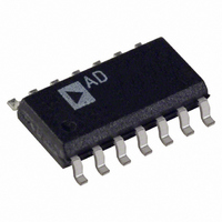
AD8522ARZ Analog Devices Inc, AD8522ARZ Datasheet - Page 2

AD8522ARZ
Manufacturer Part Number
AD8522ARZ
Description
IC DAC 12BIT DUAL 5V 14-SOIC
Manufacturer
Analog Devices Inc
Datasheet
1.AD8522ARZ.pdf
(8 pages)
Specifications of AD8522ARZ
Data Interface
Serial
Settling Time
16µs
Number Of Bits
12
Number Of Converters
2
Voltage Supply Source
Single Supply
Power Dissipation (max)
25mW
Operating Temperature
-40°C ~ 85°C
Mounting Type
Surface Mount
Package / Case
14-SOIC (3.9mm Width), 14-SOL
Resolution (bits)
12bit
Sampling Rate
62.5kSPS
Input Channel Type
Serial
Supply Voltage Range - Analog
4.5V To 5.5V
Supply Current
3mA
Digital Ic Case Style
SOIC
Package
14SOIC N
Resolution
12 Bit
Conversion Rate
62.5 KSPS
Architecture
R-2R
Digital Interface Type
Serial (3-Wire)
Number Of Outputs Per Chip
2
Output Type
Voltage
Integral Nonlinearity Error
±1.5 LSB
Maximum Settling Time
16(Typ) us
Lead Free Status / RoHS Status
Lead free / RoHS Compliant
Available stocks
Company
Part Number
Manufacturer
Quantity
Price
Company:
Part Number:
AD8522ARZ
Manufacturer:
AD
Quantity:
4 300
Part Number:
AD8522ARZ
Manufacturer:
ADI/亚德诺
Quantity:
20 000
AD8522–SPECIFICATIONS
ELECTRICAL CHARACTERISTICS
Parameter
STATIC PERFORMANCE
MATCHING PERFORMANCE
ANALOG OUTPUT
REFERENCE OUTPUT
LOGIC INPUTS & OUTPUTS
TIMING SPECIFICATIONS
AC CHARACTERISTICS
SUPPLY CHARACTERISTICS
NOTES
1
2
3
4
5
6
7
Specifications subject to change without notice.
1 LSB = 1 mV for 0 V to +4.095 V output range.
Includes internal voltage reference error.
These parameters are guaranteed by design and not subject to production testing.
Very little sink current is available at the V
All input control signals are specified with t
The settling time specification does not apply for negative going transitions within the last 6 LSBs of ground. Some devices exhibit double the typical settling time in this 6 LSB region.
Power Dissipation is calculated I
Resolution
Relative Accuracy
Differential Nonlinearity
Zero-Scale Error
Full-Scale Voltage
Full-Scale Tempco
Linearity Matching Error
Output Current
Load Regulation at Half-Scale
Capacitive Load
Output Voltage
Output Source Current
Line Rejection
Load Regulation
Logic Input Low Voltage
Logic Input High Voltage
Input Leakage Current
Input Capacitance
Logic Output Voltage Low
Logic Output Voltage High
Clock Width High
Clock Width Low
Load Pulse Width
Data Setup
Data Hold
Clear Pulse Width
Load Setup
Load Hold
Select
Deselect
Clock to SDO Propagation Delay
Voltage Output Settling Time
Crosstalk
DAC Glitch
Digital Feedthrough
Positive Supply Current
Power Dissipation
Power Supply Sensitivity
1
3
2
7
3
2, 3
DD
4
3, 5
5 V.
3, 5
6
REF
r
= t
pin. Use external buffer if setting up a virtual ground.
f
= 5 ns (10% to 90% of +5 V) and timed from a voltage level of 1.6 V.
C
Symbol
N
INL
DNL
V
V
TCV
I
LD
C
V
I
LN
LD
V
V
I
C
V
V
t
t
t
t
t
t
t
t
t
t
t
t
Q
D
I
P
PSS
CH
CL
LDW
DS
DH
CLRW
LD1
LD2
CSS
CSH
PD
S
OUT
REF
IL
DD
V
DISS
ZSE
FS
REF
IL
IH
OL
OH
L
IL
T
FT
FS
REG
REJ
REG
A/B
FS
(@ V
otherwise noted)
Condition
Monotonic
Data = 000
Data = FFF
Data = 800
R
No Oscillation
I
I
I
To 1 LSB of Final Value
Signal Measured at DAC Output,
While Changing Opposite LDA/B
Half-Scale Transition
Signal Measured at DAC Output,
While Changing Data Without LDA/B
V
V
V
V
REF
OL
OH
DD
V
V
L
DD
DD
DD
DD
REF
DD
= +5.0 V
= 402
= 1.6 mA
= 400 A
= 0 to 5 mA, Data = 800
= 5.5 V, V
= 5 V, V
= 5 V, V
= 5 V, V
= 5%
< 18 mV
H
H
H
to , Data = 800
–2–
, V
IL
IH
IL
10%, R
IH
= 0 V
= 0 V
= 2.4 V or V
OUT
= 2.4 V or V
L
= No Load, –40 C T
3 LSB
IL
H
H
IL
= 0.8 V
= 0.8 V
A
Min
12
-1.5
-1
4.079
2.484
2.4
3.5
35
35
25
10
20
20
10
10
30
30
20
+85 C, both DACs tested, unless
Typ
+0.5
4.095
1
500
2.500
0.025
0.025
45
16
38
13
2
3
1
15
5
0.002
0.5
0.5
15
1
Max
+1.5
+1
+3
4.111
3
2.516
5
0.08
0.1
0.8
10
10
0.4
80
5
2
25
10
0.004
5
Units
Bits
LSB
LSB
mV
Volts
ppm/ C
LSB
mA
LSB
pF
V
mA
%/V
%/mA
V
V
pF
V
V
ns
ns
ns
ns
ns
ns
ns
ns
ns
ns
ns
dB
nV s
nV s
mA
mA
mW
mW
%/%
A
s
REV. A


