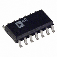
AD8522ARZ Analog Devices Inc, AD8522ARZ Datasheet - Page 6

AD8522ARZ
Manufacturer Part Number
AD8522ARZ
Description
IC DAC 12BIT DUAL 5V 14-SOIC
Manufacturer
Analog Devices Inc
Datasheet
1.AD8522ARZ.pdf
(8 pages)
Specifications of AD8522ARZ
Data Interface
Serial
Settling Time
16µs
Number Of Bits
12
Number Of Converters
2
Voltage Supply Source
Single Supply
Power Dissipation (max)
25mW
Operating Temperature
-40°C ~ 85°C
Mounting Type
Surface Mount
Package / Case
14-SOIC (3.9mm Width), 14-SOL
Resolution (bits)
12bit
Sampling Rate
62.5kSPS
Input Channel Type
Serial
Supply Voltage Range - Analog
4.5V To 5.5V
Supply Current
3mA
Digital Ic Case Style
SOIC
Package
14SOIC N
Resolution
12 Bit
Conversion Rate
62.5 KSPS
Architecture
R-2R
Digital Interface Type
Serial (3-Wire)
Number Of Outputs Per Chip
2
Output Type
Voltage
Integral Nonlinearity Error
±1.5 LSB
Maximum Settling Time
16(Typ) us
Lead Free Status / RoHS Status
Lead free / RoHS Compliant
Available stocks
Company
Part Number
Manufacturer
Quantity
Price
Company:
Part Number:
AD8522ARZ
Manufacturer:
AD
Quantity:
4 300
Part Number:
AD8522ARZ
Manufacturer:
ADI/亚德诺
Quantity:
20 000
AD8522
is possible down to +4.3 V. The minimum operating supply
voltage versus load current plot, in Figure 7, provides informa-
tion for operation below V
TIMING AND CONTROL
The AD8522 has a 16-bit serial input register that accepts
clocked in data when the CS pin is active low. The DAC regis-
ters are updated by the Load Enable (LDA and LDB) pins.
The AD8522 offers two modes of data loading. The first mode,
hardware-load, directs the data currently clocked into the serial
shift register into either the DAC A or the DAC B register or
both depending on the external active low strobing of the LDA
or LDB pin. Serial data register bit Sf/Hd must be low for this
mode to be in effect.
The second mode of operation is software-load which is de-
signed to minimize the number of control lines connected to
the AD8522. In this mode of operation the LDA and LDB pins
act as one control input taking the present contents of the serial
Typical Performance Characteristics
Figure 6. Output Swing vs. Load
5
4
3
2
1
0
–20
–40
–60
–80
10
80
60
40
20
0
Figure 9. I
100
1
LOAD RESISTANCE –
OUTPUT VOLTAGE – Volts
CURRENT
POSITIVE
LIMIT
R
DATA = FFF
R
DATA = 000
OUT
1k
L
L
TIED TO AGND
TIED TO +5V
2
vs. V
NEGATIVE
CURRENT
LIMIT
V
V
V
T
IN
IN
DD
DD
A
DATA = 800
H = +5V
L = 0V
= +25 C
H
10k
H
= +5V
OUT
= +4.5 V.
3
H
100k
Figure 7. Minimum Supply Voltage
vs. Load Current
100
90
10
0%
5.2
5.0
4.8
4.6
4.4
4.2
4.0
0.01
Figure 10. Broadband Noise
NBW = 1MHz
PROPER OPERATION
VOLTAGE IS ABOVE
WHEN V
V
DATA = FFF
T
FS
OUTPUT LOAD CURRENT – mA
A
= +25 C
0.1
1 LSB
CURVE
DD
100µs/DIV
SUPPLY
H
–6–
1.0
input register and transferring the 12 bits of data into the de-
coded address determined by the address bits A and B in the se-
rial input register.
Unipolar Output Operation
This is the basic mode of operation for the AD8522. The
AD8522 has been designed to drive loads as low as 820
parallel with 500 pF. The code table for this operation is shown
in Table III.
Hexadecimal
Number in
DAC Register
FFF
801
800
7FF
000
T
A
= +25 C
10
100
Table III. Unipolar Code Table
Figure 8. Pull-Down Voltage vs. Out-
put Sink Current Capability
Figure 11. Supply Current vs. Logic
Input Voltage
0.01
100
0.1
10
Decimal
Number in
DAC Register
4095
2049
2048
2047
0
1
9
8
7
6
5
4
3
2
1
0
1
0
V
DD
LOGIC INPUT VOLTAGE V
V
DATA = 000
V
V
= +4.5V
DD
IH
IL
OUTPUT SINK CURRENT – µA
1
= 0.0V
= 5.0V
= +5V
+85 C
10
+25 C
H
2
V
DD
–55 C
= +5V
3
100
Analog
Output
Voltage (V)
+4.095
+2.049
+2.048
+2.047
0
T
IN
A
H – Volts
= +25 C
4
REV. A
in
1000
5


