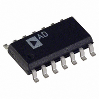
AD8522ARZ Analog Devices Inc, AD8522ARZ Datasheet - Page 4

AD8522ARZ
Manufacturer Part Number
AD8522ARZ
Description
IC DAC 12BIT DUAL 5V 14-SOIC
Manufacturer
Analog Devices Inc
Datasheet
1.AD8522ARZ.pdf
(8 pages)
Specifications of AD8522ARZ
Data Interface
Serial
Settling Time
16µs
Number Of Bits
12
Number Of Converters
2
Voltage Supply Source
Single Supply
Power Dissipation (max)
25mW
Operating Temperature
-40°C ~ 85°C
Mounting Type
Surface Mount
Package / Case
14-SOIC (3.9mm Width), 14-SOL
Resolution (bits)
12bit
Sampling Rate
62.5kSPS
Input Channel Type
Serial
Supply Voltage Range - Analog
4.5V To 5.5V
Supply Current
3mA
Digital Ic Case Style
SOIC
Package
14SOIC N
Resolution
12 Bit
Conversion Rate
62.5 KSPS
Architecture
R-2R
Digital Interface Type
Serial (3-Wire)
Number Of Outputs Per Chip
2
Output Type
Voltage
Integral Nonlinearity Error
±1.5 LSB
Maximum Settling Time
16(Typ) us
Lead Free Status / RoHS Status
Lead free / RoHS Compliant
Available stocks
Company
Part Number
Manufacturer
Quantity
Price
Company:
Part Number:
AD8522ARZ
Manufacturer:
AD
Quantity:
4 300
Part Number:
AD8522ARZ
Manufacturer:
ADI/亚德诺
Quantity:
20 000
AD8522
Pin
SDI
CLK
CS
LDA/B
SDO
RS
MSB
V
AGND
DGND
V
V
CAUTION
ESD (electrostatic discharge) sensitive device. Electrostatic charges as high as 4000 V readily
accumulate on the human body and test equipment and can discharge without detection.
Although the AD8522 features proprietary ESD protection circuitry, permanent damage may
occur on devices subjected to high energy electrostatic discharges. Therefore, proper ESD
precautions are recommended to avoid performance degradation or loss of functionality.
RS MSB
0
0
1
CS CLK
1
0
DD
REF
OUT A/B
0
1
X
X
V
AGND
DGND
OUTA
14-Pin Plastic DIP
SDO
CLK
SDI
Register Activity
Asynchronously Resets DAC Registers to Zero
Scale
Asynchronously Presets DAC Registers to
Half Scale (800
None
Shift Register
No Effect
Shifts Register One Bit, SDO Outputs Data
from 16 Clocks Earlier
CS
Serial Data Input, input data loads directly into the shift register.
Clock input, positive edge clocks data into shift register.
Chip Select, active low input. Prevents shift register loading when high. Does not affect LDA and LDB operation.
Load DAC register strobes, active low. Transfers shift register data to DAC register. See truth table for operation.
Software decode feature only requires one LD strobe. Tie LDA and LDB together or use one of them with the
other pin tied high.
Serial Data Output. Output of shift register, always active.
Resets DAC registers to condition determined by MSB pin. Active low input.
Digital input: High presets DAC registers to half scale (800
strobed to active low.
Positive +5 V power supply input. Tolerance
Analog Ground Input.
Digital Ground Input.
Reference Voltage Output, 2.5 V nominal.
DAC A/B voltage outputs, 4.095 V full scale,
Function
1
2
3
4
5
6
7
PIN CONFIGURATION
(Not To Scale)
Table II. Truth Tables
AD8522
DAC Register Preset
Shift Register
14
13
12
11
10
H
9
8
)
V
V
V
MSB
RS
LDA
LDB
OUTB
REF
DD
14-Lead SO-14
1
PIN DESCRIPTION
–4–
10%.
5 mA output.
ABSOLUTE MAXIMUM RATINGS*
V
Logic Inputs and Output to DGND . . . . . –0.3 V, V
V
V
AGND to DGND . . . . . . . . . . . . . . . . . . . . . . . . . –0.3 V, V
I
Package Power Dissipation . . . . . . . . . . . . . . . (T
Thermal Resistance,
Maximum Junction Temperature (T
Operating Temperature Range . . . . . . . . . . . . . –40 C to +85 C
Storage Temperature Range . . . . . . . . . . . . . –65 C to +150 C
Lead Temperature (Soldering, 10 sec) . . . . . . . . . . . . . +300 C
*Stresses above those listed under “Absolute Maximum Ratings” may cause
Model
AD8522AN
AD8522AR
The AD8522 contains 1482 transistors.
permanent damage to the device. This is a stress rating only and functional
operation of the device at these or any other conditions above those indicated in the
operational sections of this specification is not implied. Exposure to absolute
maximum rating conditions for extended periods may affect device reliability.
OUT
DD
OUT
REF
14-Pin Plastic DIP Package (N-14) . . . . . . . . . . . . . 83 C/W
14-Lead SOIC Package (SO-14) . . . . . . . . . . . . . . 120 C/W
to DGND & AGND . . . . . . . . . . . . . . . . . . . –0.3 V, +7 V
to AGND . . . . . . . . . . . . . . . . . . . . . –0.3 V, V
Short Circuit to GND or V
to AGND . . . . . . . . . . . . . . . . . . . . . –0.3 V, V
H
); Low clears all registers to zero (000
Temperature
Range
–40 C to +85 C
–40 C to +85 C
ORDERING GUIDE
JA
DD
WARNING!
J
. . . . . . . . . . . . . . . . 50 mA
Package
Description
14-Pin P-DIP
14-Lead SOIC SO-14
max) . . . . . . . . . . 150 C
ESD SENSITIVE DEVICE
H
), when RS is
J
max–T
DD
DD
DD
Package
Option
N-14
REV. A
+ 0.3 V
+ 0.3 V
+ 0.3 V
A
)/
DD
JA


