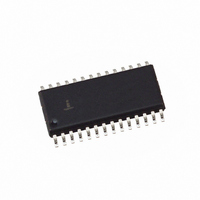
HI5741BIB Intersil, HI5741BIB Datasheet - Page 8

HI5741BIB
Manufacturer Part Number
HI5741BIB
Description
IC DAC 14-BIT 100MSPS 28-SOIC
Manufacturer
Intersil
Datasheet
1.HI5741BIB.pdf
(13 pages)
Specifications of HI5741BIB
Settling Time
20ns
Number Of Bits
14
Data Interface
Parallel
Number Of Converters
1
Voltage Supply Source
Analog and Digital, Dual ±
Power Dissipation (max)
650mW
Operating Temperature
-40°C ~ 85°C
Mounting Type
Surface Mount
Package / Case
28-SOIC (7.5mm Width)
Lead Free Status / RoHS Status
Contains lead / RoHS non-compliant
Available stocks
Company
Part Number
Manufacturer
Quantity
Price
Company:
Part Number:
HI5741BIB
Manufacturer:
HARRIS
Quantity:
91
Part Number:
HI5741BIB
Manufacturer:
INTERSIL
Quantity:
20 000
Company:
Part Number:
HI5741BIBZ
Manufacturer:
Intersil
Quantity:
126
Typical Performance Curves
Pin Descriptions
S
C
PIN NO.
17, 28
START 1.900MHz
1-14
f
FIGURE 18. TYPICAL SETTLING TIME PERFORMANCE
15
16
18
23
27
19
21
20
22
24
25
26
CLK
1
= 20 MSPS
CH1 1.00mV
FIGURE 16. TYPICAL MTPR PERFORMANCE
D13 (MSB) thru D0 (LSB) Digital Data Bit 13, the Most Significant Bit through Digital Data Bit 0, the Least Significant Bit.
CTRL AMP OUT
CTRL AMP IN
12-BIT WINDOW
∆
@
PIN NAME
: 240µV
REF OUT
: -30.96mV
~
DGND
AGND
DV
ARTN
DV
R
AV
I
I
CLK
OUT
OUT
SET
SETTLING TIME
~
CC
EE
EE
10ns
10dB/
8
M 5.0ns CH1
Data Clock Pin 100kHz to 100 MSPS.
Digital Logic Supply +5V.
Digital Ground.
-5.2V Logic Supply.
External Resistor to set the full scale output current. I
Analog Ground Supply current return pin.
Analog Signal Return for the R/2R ladder.
Current Output Pin.
Complementary Current Output pin.
-5.2V Analog Supply.
Input to the current source base rail. Typically connected to CTRL AMP OUT and a 0.1µF capacitor to AV
Allows external control of the current sources.
Control amplifier out. Provides precision control of the current sources when connected to CTRL AMP IN
such that I
-1.23V (typical) bandgap reference voltage output. Can sink up to 500µA or be overdriven by an external
reference capable of delivering up to 2mA.
(Continued)
FS
MTPR = 75.17dBc
STOP 3.100MHz
= 16 x (V
-16.9mV
REFOUT
HI5741
/R
SET
).
S
C
CENTER 26.637MHz
PIN DESCRIPTION
f
f
SFDR = 77.5dBc
1
CLK
OUT
CH1 1.00mV
= 100 MSPS
= 26.6MHz
FIGURE 19. TYPICAL GLITCH ENERGY
FIGURE 17. SFDR WITHIN A WINDOW
FS
= 16 x (V
GLITCH = (0.5) • (300µV) • (3.3ns)
∆
@
: 300µV
: -124.1mV
= 0.495pV/s
REFOUT
10dB/
/R
SET
M 5.0ns CH1
). Typically 976Ω.
September 20, 2006
SPAN 2.000MHz
-109mV
FN4071.12
EE
.


