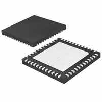
LTC2753IUK-12#TRPBF Linear Technology, LTC2753IUK-12#TRPBF Datasheet - Page 10

LTC2753IUK-12#TRPBF
Manufacturer Part Number
LTC2753IUK-12#TRPBF
Description
IC DAC 12BIT DUAL 48-QFN
Manufacturer
Linear Technology
Series
SoftSpan™r
Datasheet
1.LTC2753CUK-12PBF.pdf
(24 pages)
Specifications of LTC2753IUK-12#TRPBF
Settling Time
2µs
Number Of Bits
12
Data Interface
Parallel
Number Of Converters
2
Voltage Supply Source
Single Supply
Operating Temperature
-40°C ~ 85°C
Mounting Type
Surface Mount
Package / Case
48-QFN
Lead Free Status / RoHS Status
Lead free / RoHS Compliant
Power Dissipation (max)
-
PIN FUNCTIONS
LTC2753
R
Resistors. The 20k reference inverting resistors R1 and R2
are connected internally from R
to REFA, respectively (see Block Diagram). For normal
operation tie R
reference inverting amplifi er (see Typical Applications).
R
Resistors. The 20k resistor R1 is connected internally from
R
reference voltage V
S2 (Pin 3): Span I/O Bit 2. Pins S0, S1 and S2 are used
to program and to read back the output ranges of the
DACs.
I
I
GND (Pin 5): Shield Ground, provides necessary shielding
for I
D3-D11 (Pins 6-14): LTC2753-12 Only. DAC Input/Output
Data Bits. These I/O pins set and read back the DAC code.
D11 is the MSB.
D5-D13 (Pins 6-14): LTC2753-14 Only. DAC Input/Output
Data Bits. These I/O pins set and read back the DAC code.
D13 is the MSB.
D7-D15 (Pins 6-14): LTC2753-16 Only. DAC Input/Output
Data Bits. These I/O pins set and read back the DAC code.
D15 is the MSB.
V
Requires a 0.1μF bypass capacitor to GND.
NC (Pin 16): No Internal Connection.
A1 (Pin 17): DAC Address Bit 1. See Table 3.
A0 (Pin 18): DAC Address Bit 0. See Table 3.
GND (Pin 19): Ground. Tie to ground.
CLR (Pin 20): Asynchronous Clear. When CLR is taken
to a logic low, the data registers are reset to the zero-volt
code for the present output range (V
MSPAN (Pin 21): Manual Span Control Pin. MSPAN is used
to confi gure the LTC2753 for operation in a single, fi xed
10
OUT2A
OUT2A
DD
COM
IN
IN
(Pin 2): Input Resistor R1 of the Reference Inverting
to R
OUT2A
(Pin 15): Positive Supply Input 2.7V ≤ V
(Pin 1): Center Tap Point for the Reference Inverting
to ground.
(Pin 4): DAC A Current Output Complement. Tie
COM
. Tie to ground.
. For normal operation tie R
COM
REF
to the negative input of the external
. Typically 5V; accepts up to ±15V.
IN
to R
OUT
COM
IN
= 0V).
and from R
to the external
DD
≤ 5.5V.
COM
output range. When confi gured for single-span operation,
the output range is set via hardware pin strapping. The
input and DAC registers of the span I/O port are transparent
and do not respond to write or update commands.
To confi gure the part for single-span use, tie MSPAN directly
to V
confi guration), the output ranges are set and verifi ed by
using write, update and read operations. See Manual Span
Confi guration in the Operation section. MSPAN must be
connected either directly to GND (SoftSpan confi guration)
or V
D0-D2 (Pins 22-24): LTC2753-12 Only. DAC Input/Output
Data Bits. These I/O pins set and read back the DAC code.
D0 is the LSB.
D0-D4 (Pins 22-26): LTC2753-14 Only. DAC Input/Output
Data Bits. These I/O pins set and read back the DAC code.
D0 is the LSB.
D0-D6 (Pins 22-28): LTC2753-16 Only. DAC Input/Output
Data Bits. These I/O pins set and read back the DAC code.
D0 is the LSB.
NC (Pins 25-30): LTC2753-12 Only. No Internal Connection.
NC (Pins 27-30): LTC2753-14 Only. No Internal Connection.
NC (Pins 29, 30): LTC2753-16 Only. No Internal Con-
nection.
GND (Pin 31): Shield Ground, provides necessary shielding
for I
I
I
S0 (Pin 33): Span I/O Bit 0. Pins S0, S1 and S2 are used to
program and to read back the output range of the DACs.
D/S (Pin 34): Data/Span Select. This pin is used to select
the data I/O pins or the span I/O pins (D0 to D15 or S0
to S2, respectively), along with their respective dedicated
registers, for write or read operations. Update operations
ignore D/S, since all updates affect both data and span
registers. For single-span operation, tie D/S to ground.
READ (Pin 35): Read Pin. When READ is asserted high,
the data I/O pins (D0-D15) or span I/O pins (S0-S2)
OUT2B
OUT2B
DD
DD
OUT2B
. If MSPAN is instead connected to GND (SoftSpan
to ground.
(Pin 32): DAC B Current Output Complement. Tie
(single-span confi guration).
. Tie to ground.
2753f


