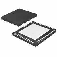
LTC2753IUK-12#TRPBF Linear Technology, LTC2753IUK-12#TRPBF Datasheet - Page 14

LTC2753IUK-12#TRPBF
Manufacturer Part Number
LTC2753IUK-12#TRPBF
Description
IC DAC 12BIT DUAL 48-QFN
Manufacturer
Linear Technology
Series
SoftSpan™r
Datasheet
1.LTC2753CUK-12PBF.pdf
(24 pages)
Specifications of LTC2753IUK-12#TRPBF
Settling Time
2µs
Number Of Bits
12
Data Interface
Parallel
Number Of Converters
2
Voltage Supply Source
Single Supply
Operating Temperature
-40°C ~ 85°C
Mounting Type
Surface Mount
Package / Case
48-QFN
Lead Free Status / RoHS Status
Lead free / RoHS Compliant
Power Dissipation (max)
-
OPERATION
LTC2753
Output Ranges
The LTC2753 is a dual current-output, parallel-input preci-
sion multiplying DAC with software-programmable output
ranges. SoftSpan provides two unipolar output ranges
(0V to 5V and 0V to 10V), and four bipolar ranges (±2.5V,
±5V, ±10V and –2.5V to 7.5V). These ranges are obtained
when an external precision 5V reference is used. When
a reference voltage of 2V is used, the SoftSpan ranges
become: 0V to 2V, 0V to 4V, ±1V, ±2V, ±4V and –1V to 3V.
The output ranges are linearly scaled for references other
than 2V and 5V.
Digital Section
The LTC2753 has 4 internal registers for each DAC, a total
of 8 registers (see Block Diagram). Each DAC channel has
two sets of double-buffered registers—one set for the data,
and one set for the span (output range) of the DAC. The
double-buffered feature provides the capability to simulta-
neously update the span and code, which allows smooth
voltage transitions when changing output ranges. It also
permits the simultaneous updating of multiple DACs.
Each set of double-buffered registers comprises an input
register and a DAC register. The input registers are holding
buffers—when data is loaded into an input register via a
write operation, the DAC outputs are not affected.
The contents of a DAC register, on the other hand, di-
rectly control the DAC output voltage or output range.
The contents of the DAC registers are changed by copying
the contents of an input register into its associated DAC
register via an update operation.
Write and Update Operations
The data input register of the addressed DAC is loaded
directly from a 16-bit microprocessor bus by holding the
D/S pin low and pulsing the WR pin low (write operation).
The DAC register is loaded by pulsing the UPD pin high
(update operation), which copies the data held in the input
register into the DAC register. Note that updates always
include both data and span; but the DAC register values
will not change unless the input register values have previ-
ously been changed via a write operation.
14
Loading the span input register is accomplished similarly,
holding the D/S pin high and bringing the WR pin low. The
span and data register structures are the same except for
the number of parallel bits—the span registers have 3 bits,
while the data registers have 12, 14, or 16.
To make both registers transparent for fl owthrough
mode, tie WR low and UPD high. However, this defeats
the deglitcher operation and output glitch impulse may
increase. The deglitcher is activated on the rising edge
of the UPD pin.
The interface also allows the use of the input and DAC
registers in a master-slave, or edge-triggered, confi gura-
tion. This mode of operation occurs when WR and UPD
are tied together and driven by a single clock signal. The
data bits are loaded into the input register on the falling
edge of the clock and then loaded into the DAC register
on the rising edge.
It is possible to control both data and span on one 16-bit
wide data bus by allowing span pins S2 to S0 to share
bus lines with the data LSBs (D2 to D0). No write or read
operation includes both span and data, so there cannot
be a confl ict.
The asynchronous clear pin resets both DACs to 0V in any
output range. CLR resets all data registers, while leaving
the span registers undisturbed.
Figure 1. Using MSPAN to Confi gure the LTC2753 for Single-Span
MSPAN
S2
S1
S0
D/S
WR
Operation (±10V Range).
UPD
V
V
DD
DD
READ
A1
DAC A
DAC B
A0
LTC2753-16
DATA I/O
16
2753 F01
2753f


