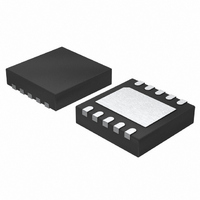
LTC2642AIDD-16#TRPBF Linear Technology, LTC2642AIDD-16#TRPBF Datasheet - Page 11

LTC2642AIDD-16#TRPBF
Manufacturer Part Number
LTC2642AIDD-16#TRPBF
Description
IC DAC 16BIT VOUT 10-DFN
Manufacturer
Linear Technology
Datasheet
1.LTC2642CDD-12PBF.pdf
(24 pages)
Specifications of LTC2642AIDD-16#TRPBF
Settling Time
1µs
Number Of Bits
16
Data Interface
Serial
Number Of Converters
1
Voltage Supply Source
Single Supply
Power Dissipation (max)
600µW
Operating Temperature
-40°C ~ 85°C
Mounting Type
Surface Mount
Package / Case
10-DFN
Lead Free Status / RoHS Status
Lead free / RoHS Compliant
Available stocks
Company
Part Number
Manufacturer
Quantity
Price
General Description
The LTC2641/LTC2642 family of 16-/14-/12-bit voltage
output DACs offer full 16-bit performance with less than
±1LSB integral linearity error and less than ±1LSB differ-
ential linearity error, guaranteeing monotonic operation.
They operate from a single supply ranging from 2.7V to
5.5V, consuming 120μA (typical). An external voltage
reference of 2V to V
output voltage. A 3-wire serial interface allows the
LTC2641/LTC2642 to fi t into a small 8-/10-pin MSOP or
DFN 3mm × 3mm package.
Digital-to-Analog Architecture
The DAC architecture is a voltage switching mode resis-
tor ladder using precision thin-fi lm resistors and CMOS
switches. The LTC2641/LTC2642 DAC resistor ladders are
composed of a proprietary arrangement of matched DAC
sections. The four MSBs are decoded to drive 15 equally
weighted segments, and the remaining lower bits drive
successively lower weighted sections. Major carry glitch
impulse is very low at 500pV•sec, C
lower than previous DACs of this type.
TIMING DIAGRAM
OPERATION
CS/LD
SCK
SDI
t
5
DD
determines the DAC’s full-scale
t
7
t
1
L
t
= 10pF, ten times
2
1
t
2
3
The digital-to-analog transfer function at the V
is:
where k is the decimal equivalent of the binary DAC input
code, N is the resolution, and V
V
The LTC2642 includes matched resistors that are tied
to an external amplifi er to provide bipolar output swing
(Figure 2). The bipolar transfer function at the RFB pin is:
(see Tables 2a, 2b and 2c).
Serial Interface
The LTC2641/LTC2642 communicates via a standard
3-wire SPI/QSPI/MICROWIRE compatible interface. The
chip select input (CS) controls and frames the loading
of serial data from the data input (DIN). Following a CS
t
4
DD
V
V
OUT(IDEAL)
(see Tables 1a, 1b and 1c).
OUT _BIPOLAR(IDEAL)
3
=
2
k
N
LTC2641/LTC2642
15
V
REF
= V
REF
REF
2
N–1
k
t
6
16
is between 2.0V and
– 1
t
8
OUT
11
26412fb
26412 TD
pin


