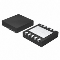
LTC2642AIDD-16#TRPBF Linear Technology, LTC2642AIDD-16#TRPBF Datasheet - Page 9

LTC2642AIDD-16#TRPBF
Manufacturer Part Number
LTC2642AIDD-16#TRPBF
Description
IC DAC 16BIT VOUT 10-DFN
Manufacturer
Linear Technology
Datasheet
1.LTC2642CDD-12PBF.pdf
(24 pages)
Specifications of LTC2642AIDD-16#TRPBF
Settling Time
1µs
Number Of Bits
16
Data Interface
Serial
Number Of Converters
1
Voltage Supply Source
Single Supply
Power Dissipation (max)
600µW
Operating Temperature
-40°C ~ 85°C
Mounting Type
Surface Mount
Package / Case
10-DFN
Lead Free Status / RoHS Status
Lead free / RoHS Compliant
Available stocks
Company
Part Number
Manufacturer
Quantity
Price
PIN FUNCTIONS
LTC2641 – MSOP, DFN Packages
REF (Pin 1): Reference Voltage Input. Apply an external
reference at REF between 2V and V
CS (Pin 2): Serial Interface Chip Select/Load Input. When
CS is low, SCLK is enabled for shifting in data on DIN.
When CS is taken high, SCLK is disabled, the 16-bit input
word is latched and the DAC is updated.
SCLK (Pin 3): Serial Interface Clock Input. CMOS and
TTL compatible.
DIN (Pin 4): Serial Interface Data Input. Data is applied
to DIN for transfer to the device at the rising edge of
SCLK.
CLR (Pin 5): Asynchronous Clear Input. A logic low clears
the DAC to code 0.
V
0V to V
V
5.5V.
GND (Pin 8): Circuit Ground.
Exposed Pad (DFN Pin 9): Circuit Ground. Must be sol-
dered to PCB ground.
LTC2641 – SO Package
V
0V to V
GND (Pin 2): Circuit Ground.
REF (Pin 3): Reference Voltage Input. Apply an external
reference at REF between 2V and V
CS (Pin 4): Serial Interface Chip Select/Load Input. When
CS is low, SCLK is enabled for shifting in data on DIN.
When CS is taken high, SCLK is disabled, the 16-bit input
word is latched and the DAC is updated.
SCLK (Pin 5): Serial Interface Clock Input. CMOS and
TTL compatible.
OUT
OUT
DD
(Pin 7): Supply Voltage. Set between 2.7V and
(Pin 6): DAC Output Voltage. The output range is
(Pin 1): DAC Output Voltage. The output range is
REF
REF
.
.
DD
DD
.
.
DIN (Pin 6): Serial Interface Data Input. Data is applied
to DIN for transfer to the device at the rising edge of
SCLK.
GND (Pin 7): Circuit Ground Pin. Must be connected to
Pin 2 (GND).
V
5.5V.
LTC2642 – MSOP , DFN Packages
REF (Pin 1): Reference Voltage Input. Apply an external
reference at REF between 2V and V
CS (Pin 2): Serial Interface Chip Select/Load Input. When
CS is low, SCLK is enabled for shifting in data on DIN.
When CS is taken high, SCLK is disabled, the 16-bit input
word is latched and the DAC is updated.
SCLK (Pin 3): Serial Interface Clock Input. CMOS and
TTL compatible.
DIN (Pin 4): Serial Interface Data Input. Data is applied
to DIN for transfer to the device at the rising edge of
SCLK.
CLR (Pin 5): Asynchronous Clear Input. A logic low clears
the DAC to midscale.
V
0V to V
INV (Pin 7): Center Tap of Internal Scaling Resistors. Con-
nect to an external amplifi er’s inverting input in bipolar
mode.
R
amplifi er’s output in bipolar mode. The bipolar output
range is –V
V
5.5V.
GND (Pin 10): Circuit Ground.
Exposed Pad (DFN Pin 11): Circuit Ground. Must be
soldered to PCB ground.
OUT
DD
DD
FB
(Pin 8): Feedback Resistor. Connect to an external
(Pin 8): Supply Voltage. Set between 2.7V and
(Pin 9): Supply Voltage. Set between 2.7V and
(Pin 6): DAC Output Voltage. The output range is
REF
.
REF
to V
REF
LTC2641/LTC2642
.
DD
.
26412fb
9


