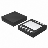
LTC2642AIDD-16#TRPBF Linear Technology, LTC2642AIDD-16#TRPBF Datasheet - Page 18

LTC2642AIDD-16#TRPBF
Manufacturer Part Number
LTC2642AIDD-16#TRPBF
Description
IC DAC 16BIT VOUT 10-DFN
Manufacturer
Linear Technology
Datasheet
1.LTC2642CDD-12PBF.pdf
(24 pages)
Specifications of LTC2642AIDD-16#TRPBF
Settling Time
1µs
Number Of Bits
16
Data Interface
Serial
Number Of Converters
1
Voltage Supply Source
Single Supply
Power Dissipation (max)
600µW
Operating Temperature
-40°C ~ 85°C
Mounting Type
Surface Mount
Package / Case
10-DFN
Lead Free Status / RoHS Status
Lead free / RoHS Compliant
Available stocks
Company
Part Number
Manufacturer
Quantity
Price
LTC2641/LTC2642
as the external reference remains stable with the added
capacative loading.
Digital Inputs and Interface Logic
All of the digital inputs include Schmitt-trigger buffers
to accept slow transition interfaces. This means that op-
tocuplers can interface directly to the LTC2641/LTC2642
without additional external logic. Digital input hysteresis
is typically 150mV.
The digital inputs are compatible with TTL/CMOS-logic
levels. However, rail-to-rail (CMOS) logic swings are
preferred, because operating the logic inputs away from
the supply rails generates additional I
(see Typical Performance Characteristic graph Supply
Current vs Logic Input Voltage).
Digital feedthrough is only 0.2nV•s typical, but it is always
preferred to keep all logic inputs static except when loading
a new code into the DAC.
Board Layout for Precision
Even a small amount of board leakage can degrade ac-
curacy. The 6nA leakage current into V
generate 1LSB offset error corresponds to 833MΩ leakage
resistance from a 5V supply.
The V
coupling, so minimum trace length, appropriate shielding
and clean board layout are imperative here.
Temperature differences at the DAC, op amp or reference
pins can easily generate tens of microvolts of thermo-
couple voltages. Analog signal traces should be short,
close together and away from heat dissipating compo-
nents. Air currents across the board can also generate
thermocouples.
The PC board should have separate areas for the analog and
digital sections of the circuit. A single, solid ground plane
APPLICATIONS INFORMATION
18
OUT
node is relatively sensitive to capacitive noise
DD
and GND current,
OUT
needed to
should be used, with analog and digital signals carefully
routed over separate areas of the plane. This keeps digital
signals away from sensitive analog signals and minimizes
the interaction between digital ground currents and the
analog section of the ground plane.
A “star ground” area should be established by attaching
the LTC2641/LTC2642 GND pin, V
V
GND plane. Care should be taken to ensure that no large
GND return current paths fl ow through the “star GND”
area. In particular, the resistance from the LTC2641 GND
pin to the point where the V
the ground plane should be as low as possible. Excessive
resistance here will be multiplied by the code dependent
I
produced by V
the S8 package both GND pins, Pin 2 and Pin 7 should
be tied to the same GND plane.
Sources of ground return current in the analog area include
op amp power supply bypass capacitors and the GND
connection for single supply amps. A useful technique
for minimizing errors is to use a separate board layer
for power ground return connections, and reserve one
ground plane layer for low current “signal” GND connec-
tions. The “signal”, or “star” GND plane must connected
to the “power” GND plane at a single point, which should
be located near the LTC2641/LTC2642 GND pin.
If separate analog and digital ground areas exist it is neces-
sary to connect them at a single location, which should be
fairly close to the DAC for digital signal integrity. In some
systems, large GND return currents can fl ow between the
digital and analog GNDs, especially if different PC boards
are involved. In such cases the digital and analog ground
connection point should not be made right at the “star”
GND area, so the highly sensitive analog signals are not
corrupted. If forced to choose, always place analog ground
quality ahead of digital signal ground. (A few mV of noise
REF
OUT
current to produce an INL error similar to the error
GND reference terminal to the same area on the
REF
source resistance. For the LTC2641 in
REF
input source connects to
REF
GND and the DAC
26412fb


