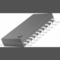
CS4351-DZZ Cirrus Logic Inc, CS4351-DZZ Datasheet - Page 18

CS4351-DZZ
Manufacturer Part Number
CS4351-DZZ
Description
IC DAC STER 112DB 192KHZ 20TSSOP
Manufacturer
Cirrus Logic Inc
Datasheet
1.CS4351-CZZ.pdf
(37 pages)
Specifications of CS4351-DZZ
Data Interface
Serial
Number Of Bits
24
Number Of Converters
2
Voltage Supply Source
Analog and Digital
Power Dissipation (max)
354mW
Operating Temperature
-40°C ~ 85°C
Mounting Type
Surface Mount
Package / Case
20-TSSOP
Resolution (bits)
24bit
Sampling Rate
192kSPS
Input Channel Type
Serial
Supply Current
15mA
Digital Ic Case Style
TSSOP
No. Of Pins
20
Lead Free Status / RoHS Status
Lead free / RoHS Compliant
For Use With
598-1152 - BOARD EVAL FOR CS4351 DAC
Settling Time
-
Lead Free Status / RoHS Status
Lead free / RoHS Compliant, Lead free / RoHS Compliant
Available stocks
Company
Part Number
Manufacturer
Quantity
Price
Company:
Part Number:
CS4351-DZZR
Manufacturer:
CIRRUSLOGIC
Quantity:
2 549
18
4.4.1
4.4.2
4.5
4.5.1
4.5.2
4.6
4.6.1
Recommended Power-Up Sequence
Popguard
The CS4351 uses a novel technique to minimize the effects of output transients during power-up and power-
down. This technology, when used with external DC-blocking capacitors in series with the audio outputs,
minimizes the audio transients commonly produced by single-ended single-supply converters. It is activated
inside the DAC when the RST pin is toggled and requires no other external control, aside from choosing the
appropriate DC-blocking capacitors.
Stand-Alone Mode
When pulled to VL the DEM pin activates the 44.1 kHz de-emphasis filter. When pulled to GND the DEM
pin turns off the de-emphasis filter.
Control Port Mode
The Mode Control bits selects either the 32, 44.1, or 48 kHz de-emphasis filter. Please see
for the desired de-emphasis control.
Stand-Alone Mode
1. Hold RST low until the power supplies and configuration pins are stable, and the master and left/right
2. Bring RST high. The device will remain in a low power state with VQ low and will initiate the Stand-
Control Port Mode
1. Hold RST low until the power supply is stable, and the master and left/right clocks are locked to the
2. Bring RST high. The device will remain in a low power state with VQ low.
3. Perform a control port write to the CP_EN bit prior to the completion of approximately 512 LRCK
4. Set the PDN bit to 0. This will initiate the power-up sequence, which lasts approximately 50 µs when
Power-Up
When the device is initially powered-up, the audio outputs, AOUTA and AOUTB, are clamped to GND.
Following a delay of approximately 1000 sample periods, each output begins to ramp toward the quies-
cent voltage. Approximately 10,000 LRCK cycles later, the outputs reach V
This gradual voltage ramping allows time for the external DC-blocking capacitors to charge to the quies-
cent voltage, minimizing audible power-up transients.
clocks are locked to the appropriate frequencies, as discussed in
port is reset to its default settings, VQ will remain low, and VBIAS will be connected to VA.
Alone power-up sequence after approximately 512 LRCK cycles in Single-Speed Mode (1024 LRCK
cycles in Double-Speed Mode, and 2048 LRCK cycles in Quad-Speed Mode).
appropriate frequencies, as discussed in
default settings, VQ will remain low, and VBIAS will be connected to VA.
cycles in Single-Speed Mode (1024 LRCK cycles in Double-Speed Mode, and 2048 LRCK cycles in
Quad-Speed Mode). The desired register settings can be loaded while keeping the PDN bit set to 1.
the POPG bit is set to 0. If the POPG bit is set to 1, see
power-up timing.
®
Transient Control
Section
4.2. In this state, the control port is reset to its
Section 4.6
Section
for a complete description of
4.2. In this state, the control
Q
and audio output begins.
Section 6.2.2
CS4351
DS566F1


