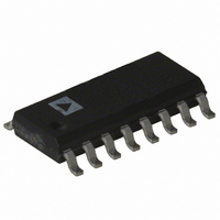
AD8803ARZ Analog Devices Inc, AD8803ARZ Datasheet - Page 8

AD8803ARZ
Manufacturer Part Number
AD8803ARZ
Description
IC DAC 8BIT OCTAL W/SD 16-SOIC
Manufacturer
Analog Devices Inc
Series
TrimDAC®r
Datasheet
1.AD8801ARZ-REEL.pdf
(16 pages)
Specifications of AD8803ARZ
Data Interface
Serial
Settling Time
600ns
Number Of Bits
8
Number Of Converters
8
Voltage Supply Source
Single Supply
Power Dissipation (max)
27.5mW
Operating Temperature
-40°C ~ 85°C
Mounting Type
Surface Mount
Package / Case
16-SOIC (3.9mm Width)
Resolution (bits)
8bit
Sampling Rate
1.7MSPS
Input Channel Type
Serial
Supply Voltage Range - Analog
2.7V To 5.5V
Supply Current
1mA
Digital Ic Case Style
SOIC
Lead Free Status / RoHS Status
Lead free / RoHS Compliant
Lead Free Status / RoHS Status
Lead free / RoHS Compliant, Lead free / RoHS Compliant
Available stocks
Company
Part Number
Manufacturer
Quantity
Price
Part Number:
AD8803ARZ
Manufacturer:
ADI/亚德诺
Quantity:
20 000
AD8801/AD8803
APPLICATIONS
Supply Bypassing
Precision analog products, such as the AD8801/AD8803, re-
quire a well filtered power source. Since the AD8801/AD8803
operate from a single +3 V to +5 V supply, it seems convenient
to simply tap into the digital logic power supply. Unfortunately,
the logic supply is often a switch-mode design, which generates
noise in the 20 kHz to 1 MHz range. In addition, fast logic gates
can generate glitches hundred of millivolts in amplitude due to
wiring resistances and inductances.
If possible, the AD8801/AD8803 should be powered directly
from the system power supply. This arrangement, shown in Fig-
ure 21, will isolate the analog section from the logic switching
transients. Even if a separate power supply trace is not available,
however, generous supply bypassing will reduce supply-line in-
duced errors. Local supply bypassing consisting of a 10 F tan-
talum electrolytic in parallel with a 0.1 F ceramic capacitor is
recommended (Figure 22).
Figure 21. Use Separate Traces to Reduce Power Supply
Noise
Figure 19. Full-Scale Error Accelerated by Burn-In
–0.02
–0.04
0.04
0.02
0
0
POWER SUPPLY
TTL/CMOS
CIRCUITS
LOGIC
+5V
150
HOURS OF OPERATION AT 150 C
x + 2
x – 2
x
+
TANT
10µF
300
0.1µF
V
V
SS = 162 PCS
450
DD
REF
AD8801/
AD8803
= +4.5V
= +4.5V
600
–8–
Figure 22. Recommended Supply Bypassing for the
AD8801/AD8803
Buffering the AD8801/AD8803 Output
In many cases, the nominal 5 k output impedance of the
AD8801/AD8803 is sufficient to drive succeeding circuitry. If a
lower output impedance is required, an external amplifier can
be added. Several examples are shown in Figure 23. One ampli-
fier of an OP291 is used as a simple buffer to reduce the output
resistance of DAC A. The OP291 was chosen primarily for its
rail-to-rail input and output operation, but it also offers opera-
tion to less than 3 V, low offset voltage, and low supply current.
The next two DACs, B and C, are configured in a summing ar-
rangement where DAC C provides the coarse output voltage
setting and DAC B can be used for fine adjustment. The inser-
tion of R1 in series with DAC B attenuates its contribution to
the voltage sum node at the DAC C output.
Figure 20. REF Input Resistance Accelerated by Burn-In
–0.5
–1.0
1.0
0.5
0
0
+
10µF
150
HOURS OF OPERATION AT 150 C
x + 2
x – 2
x
0.1µF
300
AD8801/
AD8803
DGND
V
+5V
DD
V
V
CODE = 55
SS = 162 PCS
450
DD
REF
= +4.5V
= +4.5V
H
600
REV. A


