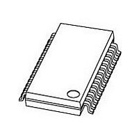
UDA1345TS NXP Semiconductors, UDA1345TS Datasheet - Page 9

UDA1345TS
Manufacturer Part Number
UDA1345TS
Description
Manufacturer
NXP Semiconductors
Datasheet
1.UDA1345TS.pdf
(29 pages)
Specifications of UDA1345TS
Single Supply Voltage (typ)
3V
Single Supply Voltage (min)
2.4V
Single Supply Voltage (max)
3.6V
Package Type
SSOP
Lead Free Status / Rohs Status
Compliant
Available stocks
Company
Part Number
Manufacturer
Quantity
Price
Company:
Part Number:
UDA1345TS
Manufacturer:
NXP
Quantity:
3 008
Part Number:
UDA1345TS
Manufacturer:
PHI
Quantity:
20 000
Company:
Part Number:
UDA1345TS/N2
Manufacturer:
NXP
Quantity:
180
Company:
Part Number:
UDA1345TS/N2
Manufacturer:
NXP
Quantity:
166
Part Number:
UDA1345TS/N2
Manufacturer:
PHILIPS/飞利浦
Quantity:
20 000
Company:
Part Number:
UDA1345TS/N2,112
Manufacturer:
ON
Quantity:
12 000
Part Number:
UDA1345TS/N2,118
Manufacturer:
NXP/恩智浦
Quantity:
20 000
NXP Semiconductors
Table 2 Digital decimation filter characteristics
Note: the digital output level is inversely proportional to the
ADC analog power supply. This means that with a
constant analog input level and increasing power supply
the digital output level will decrease proportionally.
7.4
The digital filter interpolates from 1 to 128f
cascade of a recursive filter and an FIR filter.
Table 3 Digital interpolation filter characteristics
7.5
Since the device supports a sampling range of
8 to 100 kHz, the device can support double speed (e.g.
for 44.1 kHz and 48 kHz sampling frequency) by just
doubling the system speed. In double speed all features
are available.
7.6
The 3rd-order noise shaper operates at 128f
in-band quantization noise to frequencies well above the
audio band. This noise shaping technique enables high
signal-to-noise ratios to be achieved. The noise shaper
output is converted into an analog signal using a filter
stream digital-to-analog converter.
2002 May 28
Pass-band ripple
Stop band
Dynamic range
Overall gain when
a 0 dB signal is
input to ADC to
digital output
Passband ripple
Stopband
Dynamic range
Gain
Economy audio CODEC
Interpolation filter (DAC)
Double speed
Noise shaper (DAC)
ITEM
ITEM
CONDITIONS
CONDITIONS
0 − 0.45f
0 − 0.45f
0 − 0.45f
0 − 0.45f
>0.55f
>0.55f
DC
DC
s
s
s
s
s
s
s
VALUE (dB)
VALUE (dB)
by means of a
s
. It shifts
±0.05
−1.16
±0.03
116.5
−3.5
−60
114
−65
9
7.7
The FSDAC is a semi-digital reconstruction filter that
converts the 1-bit data stream of the noise shaper to an
analog output voltage. The filter coefficients are
implemented as current sources and are summed at virtual
ground of the output operational amplifier. In this way very
high signal-to-noise performance and low clock jitter
sensitivity is achieved. A post filter is not needed due to the
inherent filter function of the DAC. On-board amplifiers
convert the FSDAC output current to an output voltage
signal capable of driving a line output.
The output voltage of the FSDAC is scaled proportionally
with the power supply voltage.
7.8
In the event that the DAC is powered-up or powered-down,
a cosine roll-off mute will be performed (when powering
down) or a cosine roll-up de-mute (when powering up) will
be performed. This is in order to prevent clicks when
powering up or down. This power-on/off mute takes
32 × 4 = 128 samples.
7.9
The UDA1345TS can be used under L3 microcontroller
interface mode or under static pin control. The mode can
be set via the Mode Control (MC) pins MC1 (pin 8) and
MC2 (pin 21). The function of these pins is given in
Table 4.
Table 4 Mode Control pins MC1 and MC2
Important: in L3MODE the UDA1345TS is completely pin
and function compatible with the UDA1340M and the
UDA1344TS.
Note: the UDA1345TS does NOT support bass-boost and
treble.
L3MODE
Test modes
Static pin mode
MODE
The Filter Stream DAC (FSDAC)
Power control
L3MODE or static pin control
HIGH
HIGH
LOW
LOW
MC2
UDA1345TS
Product specification
HIGH
HIGH
LOW
LOW
MC1


