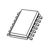
HTRC11001T/03EE,118 NXP Semiconductors, HTRC11001T/03EE,118 Datasheet - Page 13

HTRC11001T/03EE,118
Manufacturer Part Number
HTRC11001T/03EE,118
Description
Manufacturer
NXP Semiconductors
Datasheet
1.HTRC11001T03EE118.pdf
(20 pages)
Specifications of HTRC11001T/03EE,118
Operating Supply Voltage (typ)
5V
Operating Supply Voltage (min)
4.5V
Operating Supply Voltage (max)
5.5V
Operating Temp Range
-40C to 85C
Operating Temperature Classification
Industrial
Mounting
Surface Mount
Pin Count
14
Lead Free Status / Rohs Status
Compliant
Philips Semiconductors
9
In accordance with the Absolute Maximum Rating System (IEC 60134); note 1.
Note
1. Stress above one or more of the limiting values may cause permanent damage to the device. These are stresses
10 DC CHARACTERISTICS
All voltages are measured with respect to ground (pin V
Note
1. Power consumption of external quartz or any other component is not included.
2001 Nov 23
V
V
V
T
T
Supply
V
I
I
I
Driver outputs (pins TX1 and TX2)
I
R
Demodulator input (pin RX)
V
V
V
R
Digital inputs
V
V
Digital outputs
V
I
SYMBOL
SYMBOL
DD
idle
pd
ant(p)
OL
j(max)
stg
n
n(max)
RX
DD
I
diag
QGND
IH
IL
OL
o
i
HITAG reader chip
ratings only and operation of the device at these or at any other conditions above those given in Chapter 10 not
implied. Exposure or limiting values for extended periods may affect device reliability.
LIMITING VALUES
voltage at any pin (except pin RX)
maximum voltage at any pin with respect to V
voltage at pin RX
maximum junction temperature
storage temperature
supply voltage
supply current
idle current
power-down current
antenna driver output current
(peak value)
output resistance
input voltage
diagnosis level voltage
potential on pin QGND
internal demodulator
impedance
HIGH-level input voltage
LOW-level input voltage
LOW-level output voltage
LOW-level output current
PARAMETER
PARAMETER
V
V
V
permanent
pulse load; t
ratio on : off = 1 : 4
both drivers together
with respect to pin QGND
with respect to pin QGND;
V
I
V
OL(max)
DD
DD
DD
DD
OL
= 5.5 V; I
= 5.5 V; note 1
= 5.5 V
= 5 V
0.4 V
CONDITIONS
= 1 mA
SS
on
TX1
); T
< 400 ms;
DD
13
= I
(except pin RX)
amb
TX2
= 40 to +85 C
= 0
4.5
0.35V
17
0.7V
1
8
1.5
0.3
MIN.
DD
DD
5.0
4
0.2
7
2.5
0.42V
25
1.15
0.3
0.3
10
65
TYP.
MIN.
DD
HTRC11001T
5.5
10
0.4
20
200
400
7
+8
0.50V
33
V
0.3V
0.4
V
+12
140
+125
0.8
Product specification
DD
6.5
DD
MAX.
MAX.
+ 0.3 V V
DD
+ 0.3 V
DD
V
V
V
mA
mA
mA
mA
V
V
V
k
V
V
mA
C
C
UNIT
UNIT
A


