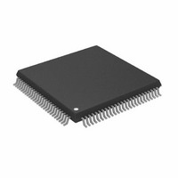
AD5382BSTZ-5 Analog Devices Inc, AD5382BSTZ-5 Datasheet - Page 11

AD5382BSTZ-5
Manufacturer Part Number
AD5382BSTZ-5
Description
IC DAC 14BIT 32CH 5V 100-LQFP
Manufacturer
Analog Devices Inc
Datasheet
1.AD5382BSTZ-5.pdf
(40 pages)
Specifications of AD5382BSTZ-5
Data Interface
Serial, Parallel
Design Resources
32 Channels of Programmable Voltage with Excellent Temperature Drift Performance Using AD5382 (CN0011) AD5382 Channel Monitor Function (CN0012)
Settling Time
8µs
Number Of Bits
14
Number Of Converters
32
Voltage Supply Source
Single Supply
Power Dissipation (max)
65mW
Operating Temperature
-40°C ~ 85°C
Mounting Type
Surface Mount
Package / Case
100-LQFP
Resolution (bits)
14bit
Sampling Rate
125kSPS
Input Channel Type
Parallel, Serial
Supply Voltage Range - Analogue
4.5V To 5.5V
Supply Voltage Range -
RoHS Compliant
Number Of Channels
32
Resolution
14b
Conversion Rate
125KSPS
Single Supply Voltage (typ)
5V
Dual Supply Voltage (typ)
Not RequiredV
Architecture
Resistor-String
Power Supply Type
Analog and Digital
Power Supply Requirement
Analog and Digital
Output Type
Voltage
Integral Nonlinearity Error
±4+/- LSB
Single Supply Voltage (min)
4.5V
Single Supply Voltage (max)
5.5V
Dual Supply Voltage (min)
Not RequiredV
Dual Supply Voltage (max)
Not RequiredV
Operating Temp Range
-40C to 85C
Operating Temperature Classification
Industrial
Mounting
Surface Mount
Pin Count
100
Package Type
LQFP
Lead Free Status / RoHS Status
Lead free / RoHS Compliant
For Use With
EVAL-AD5382EB - BOARD EVAL FOR AD5382
Lead Free Status / Rohs Status
Compliant
Available stocks
Company
Part Number
Manufacturer
Quantity
Price
Company:
Part Number:
AD5382BSTZ-5
Manufacturer:
Analog Devices Inc
Quantity:
10 000
Part Number:
AD5382BSTZ-5
Manufacturer:
ADI/亚德诺
Quantity:
20 000
PARALLEL INTERFACE
DVDD = 2.7 V to 5.5 V; AVDD = 4.5 V to 5.5 V or 2.7 V to 3.6 V; AGND = DGND = 0 V; all specifications Tmin to Tmax,
unless otherwise noted.
Table 8.
Parameter
t
t
t
t
t
t
t
t
t
t
t
t
t
t
t
t
t
t
t
t
t
1
2
3
4
5
0
1
2
3
4
5
6
7
8
9
10
11
12
13
14
15
16
17
18
19
20
Guaranteed by design and characterization, not production tested.
All input signals are specified with t
See Figure 7.
See Figure 29.
Measured with the load circuit of Figure 2.
4
4
4, 5
1, 2, 3
Limit at T
4.5
4.5
20
20
0
0
4.5
4.5
20
700
30
670
30
20
100
20
0
100
8
20
35
R
= t
R
MIN
= 5 ns (10% to 90% of DV
, T
MAX
Unit
ns min
ns min
ns min
ns min
ns min
ns min
ns min
ns min
ns min
ns min
ns max
ns max
ns min
ns min
ns max
ns min
ns min
ns min
μs typ
ns min
μsmax
DD
) and timed from a voltage level of 1.2 V.
Rev. B | Page 11 of 40
Description
REG0, REG1, address to WR rising edge setup time
REG0, REG1, address to WR rising edge hold time
CS pulse width low
WR pulse width low
CS to WR falling edge setup time
WR to CS rising edge hold time
Data to WR rising edge setup time
Data to WR rising edge hold time
WR pulse width high
Minimum WR cycle time (single-channel write)
WR rising edge to BUSY falling edge
BUSY pulse width low (single-channel update)
WR rising edge to LDAC falling edge
LDAC pulse width low
BUSY rising edge to DAC output response time
LDAC rising edge to WR rising edge
BUSY rising edge to LDAC falling edge
LDAC falling edge to DAC output response time
DAC output settling time
CLR pulse width low
CLR pulse activation time
AD5382


