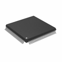
AD5382BSTZ-5 Analog Devices Inc, AD5382BSTZ-5 Datasheet - Page 26

AD5382BSTZ-5
Manufacturer Part Number
AD5382BSTZ-5
Description
IC DAC 14BIT 32CH 5V 100-LQFP
Manufacturer
Analog Devices Inc
Datasheet
1.AD5382BSTZ-5.pdf
(40 pages)
Specifications of AD5382BSTZ-5
Data Interface
Serial, Parallel
Design Resources
32 Channels of Programmable Voltage with Excellent Temperature Drift Performance Using AD5382 (CN0011) AD5382 Channel Monitor Function (CN0012)
Settling Time
8µs
Number Of Bits
14
Number Of Converters
32
Voltage Supply Source
Single Supply
Power Dissipation (max)
65mW
Operating Temperature
-40°C ~ 85°C
Mounting Type
Surface Mount
Package / Case
100-LQFP
Resolution (bits)
14bit
Sampling Rate
125kSPS
Input Channel Type
Parallel, Serial
Supply Voltage Range - Analogue
4.5V To 5.5V
Supply Voltage Range -
RoHS Compliant
Number Of Channels
32
Resolution
14b
Conversion Rate
125KSPS
Single Supply Voltage (typ)
5V
Dual Supply Voltage (typ)
Not RequiredV
Architecture
Resistor-String
Power Supply Type
Analog and Digital
Power Supply Requirement
Analog and Digital
Output Type
Voltage
Integral Nonlinearity Error
±4+/- LSB
Single Supply Voltage (min)
4.5V
Single Supply Voltage (max)
5.5V
Dual Supply Voltage (min)
Not RequiredV
Dual Supply Voltage (max)
Not RequiredV
Operating Temp Range
-40C to 85C
Operating Temperature Classification
Industrial
Mounting
Surface Mount
Pin Count
100
Package Type
LQFP
Lead Free Status / RoHS Status
Lead free / RoHS Compliant
For Use With
EVAL-AD5382EB - BOARD EVAL FOR AD5382
Lead Free Status / Rohs Status
Compliant
Available stocks
Company
Part Number
Manufacturer
Quantity
Price
Company:
Part Number:
AD5382BSTZ-5
Manufacturer:
Analog Devices Inc
Quantity:
10 000
Part Number:
AD5382BSTZ-5
Manufacturer:
ADI/亚德诺
Quantity:
20 000
AD5382
AD5382 INTERFACES
The AD5382 contains both parallel and serial interfaces.
Furthermore, the serial interface can be programmed to
be either SPI-, DSP-, MICROWIRE-, or I
SER/ PAR pin selects parallel and serial interface modes.
In serial mode, the SPI /I
MICROWIRE, or I
The device uses an internal FIFO memory to allow high speed
successive writes in parallel interface mode. The user can con-
tinue writing new data to the device while write instructions are
being executed. The BUSY signal indicates the current status of
the device, going low while instructions in the FIFO are being
executed. In parallel mode, up to 128 successive instructions
can be written to the FIFO at maximum speed. When the FIFO
is full, further writes to the device are ignored.
To minimize both the power consumption of the device and
the on-chip digital noise, the active interface powers up fully
when only the device is being written to, that is, on the falling
edge of WR or the falling edge of SYNC .
DSP-, SPI-, MICROWIRE-COMPATIBLE SERIAL
INTERFACES
The serial interface can be operated with a minimum of three
wires in standalone mode or four wires in daisy-chain mode.
Daisy chaining allows many devices to be cascaded together to
increase system channel count. The SER/ PAR pin must be tied
high and the SPI /I
the DSP-, SPI-, MICROWIRE-compatible serial interface. In
serial interface mode, the user does not need to drive the
parallel input data pins. The serial interface’s control pins are as
follows:
Table 19. 32-Channel, 14-Bit DAC Serial Input Register Configuration
MSB
A/B
SYNC , DIN, SCLK—Standard 3-wire interface pins.
DCEN—Selects standalone mode or daisy-chain mode.
SDO—Data out pin for daisy-chain mode.
R/W
0
A4
2
2
C pin (Pin 97) should be tied low to enable
C interface mode.
A3
2
C pin is used to select DSP, SPI,
A2
A1
A0
REG1
2
C-compatible. The
REG0
DB13
Rev. B | Page 26 of 40
DB12
DB11
Figure 3 and Figure 5 show timing diagrams for a serial write to
the AD5382 in standalone and daisy-chain modes. The 24-bit
data-word format for the serial interface is shown in Table 19.
A /B. When toggle mode is enabled, this pin selects whether the
data write is to the A or B register. With toggle disabled, this bit
should be set to 0 to select the A data register.
R/ W is the read or write control bit.
A4–A0 are used to address the input channels.
REG1 and REG0 select the register to which data is written, as
shown in Table 11.
DB13–DB0 contain the input data-word.
X is a don’t care condition.
Standalone Mode
By connecting the DCEN (daisy-chain enable) pin low, stand-
alone mode is enabled. The serial interface works with both a
continuous and a noncontinuous serial clock. The first falling
edge of SYNC starts the write cycle and resets a counter that
counts the number of serial clocks to ensure that the correct
number of bits are shifted into the serial shift register. Any
further edges on SYNC except for a falling edge are ignored
until 24 bits are clocked in. Once 24 bits are shifted in, the
SCLK is ignored. For another serial transfer to take place, the
counter must be reset by the falling edge of SYNC .
DB10
DB9
DB8
DB7
DB6
DB5
DB4
DB3
DB2
DB1
LSB
DB0


