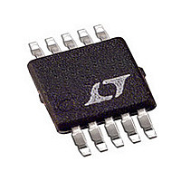
LTC4212CMSTR Linear Technology, LTC4212CMSTR Datasheet - Page 9

LTC4212CMSTR
Manufacturer Part Number
LTC4212CMSTR
Description
Manufacturer
Linear Technology
Datasheet
1.LTC4212CMSTR.pdf
(24 pages)
Specifications of LTC4212CMSTR
Linear Misc Type
Positive Low Voltage
Family Name
LTC4212
Package Type
MSOP
Operating Supply Voltage (min)
2.5V
Operating Supply Voltage (max)
16.5V
Operating Temperature (min)
0C
Operating Temperature (max)
70C
Operating Temperature Classification
Commercial
Product Depth (mm)
3mm
Product Height (mm)
0.86mm
Product Length (mm)
3mm
Mounting
Surface Mount
Pin Count
10
Lead Free Status / Rohs Status
Not Compliant
BLOCK DIAGRA
PI FU CTIO S
FAULT (Pin 10): Open Drain FAULT Output or External
FAULT Input. If the FAST COMP, SLOW COMP or the
power good circuit trips the ECB, the FAULT pin is latched
low. The FAULT pin is an open drain output and is typically
TIMER
U
ON
1
2
0.455V
1.316V
2 A
U
M6
–
+
–
+
COMP1
COMP2
V
CC
0.2V
V
REF
U
120 s
10 s
+
–
+
–
COMP3
COMP4
W
t
DELAY
1.5 s
TIMER
PULLDOWN
200 A
NORMAL
GATE
RESET
ECB
UVLO
V
REF
–
COMP5
V
CC
VALID
GLITCH
4
+
9
GLITCH FILTER
PGF
+
M5
SLOW
COMP
18 S
5 A
–
+
–
50mV
DISABLE
GLITCH
FILTER
6
+
+
SENSE
DELAY
COMP8
COMP
500ns
PGI
FAST
0.65V
V
–
+
–
–
REF
8
connected by a 10k pull-up resistor to V
circuit can also trip the ECB by driving FAULT below
1.236V (typical).
150mV
LOGIC
0.95V
M8
M3
CB
TRIPS
OR UVLO
COMP7
M9
–
COMP9
–
+
ON LOW
>10 s
200 A
GATE
3
0.2V
+
PGT
M12
7
REGULATOR
DISABLE
START-UP
CURRENT
TIMER
10 A
10 A
5 A
V
M10
Z
M1
(TYP) = 12V
CHARGING
CHARGE
PUMP
GATE
5 A
CB TRIPS
Z1
1.236V
V
V
REF
0.2V
CC
COMP6
=
+
–
Z2
V
LTC4212
CC
Z
BG
(TYP) = 28V
. An external
V
M2
REF
0.95V
0.65V
4212 BD
FAULT
10
GND
5
9
4212f


