HI5628/6IN Intersil, HI5628/6IN Datasheet
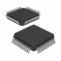
DAC DUAL 8BIT 60MSPS 48LQFP

HI5628/6IN

Manufacturer Part Number
HI5628/6IN
Description
DAC DUAL 8BIT 60MSPS 48LQFP
Manufacturer
Intersil
Datasheet

Specifications of HI5628/6IN

Settling Time
1.5µs
Number Of Bits
8
Data Interface
Parallel
Number Of Converters
2
Voltage Supply Source
Analog and Digital
Power Dissipation (max)
330mW
Operating Temperature
-40°C ~ 85°C
Mounting Type
Surface Mount
Package / Case
48-LQFP
Lead Free Status / RoHS Status
Contains lead / RoHS non-compliant

Available stocks

Company
Part Number
Manufacturer
Quantity
Price
Part Number:
HI5628/6IN
Manufacturer:
ATMEL
Quantity:
1 100
Part Number:
HI5628/6IN
Manufacturer:
Intersil
Quantity:
10 000
Part Number:
HI5628/6IN
Manufacturer:
INTERSIL
Quantity:
20 000
Part Number:
HI5628/6IN-T
Manufacturer:
Intersil
Quantity:
10 000
Part Number:
HI5628/6INZ
Manufacturer:
Intersil
Quantity:
10 000
8-Bit, 125/60MSPS, Dual High Speed
CMOS D/A Converter
The HI5628 is an 8-bit, dual 125MSPS D/A converter which
is implemented in an advanced CMOS process. Operating
from a single +5V to +3V supply, the converter provides
20.48mA of full scale output current and includes an input
data register. Low glitch energy and excellent frequency
domain performance are achieved using a segmented
architecture. The single DAC version is the HI5660 while
10-bit versions exist in the HI5760 and HI5728.
Ordering Information
HI5628IN
HI5628/6IN
HI5628EVAL1
NUMBER
PART
-40 to 85 48 Ld LQFP
RANGE
TEMP.
(
o
25
C)
Evaluation Platform
®
PACKAGE
1
Data Sheet
Q48.7x7A 125MHz
Q48.7x7A 60MHz
PKG. NO.
125MHz
CLOCK
SPEED
MAX
1-888-INTERSIL or 321-724-7143
CAUTION: These devices are sensitive to electrostatic discharge; follow proper IC Handling Procedures.
ID0 (LSB)
SLEEP
DGND
DGND
DGND
DV
AV
NC
ID4
ID3
ID2
ID1
DD
DD
Features
• Throughput Rate . . . . . . . . . . . . . . . . . . . . . . . 125MSPS
• Low Power . . . . . . . . . . . . . 330mW at 5V, 170mW at 3V
• Integral Linearity Error . . . . . . . . . . . . . . . . . . . ±0.25 LSB
• Differential Linearity . . . . . . . . . . . . . . . . . . . . . ±0.25 LSB
• Channel Isolation (Typ) . . . . . . . . . . . . . . . . . . . . . . 80dB
• SFDR to Nyquist at 10MHz Output . . . . . . . . . . . . 60dBc
• Internal 1.2V Bandgap Voltage Reference
• Single Power Supply from +5V to +3V
• CMOS Compatible Inputs
• Excellent Spurious Free Dynamic Range
Applications
• Direct Digital Frequency Synthesis
• Wireless Communications
• Signal Reconstruction
• Arbitrary Waveform Generators
• Test Equipment
• High Resolution Imaging Systems
Pinout
September 2000
10
11
12
1
2
3
4
5
6
7
8
9
All other trademarks mentioned are the property of their respective owners.
13 14 15 16
48
|
Intersil (and design) is a registered trademark of Intersil Americas Inc.
47
46
45
Copyright © Intersil Americas Inc. 2004. All Rights Reserved
44
17
HI5628 (LQFP)
43
18
TOP VIEW
42
19
41
20
40
21
22
39
38
23
37
24
36
35
34
33
32
31
30
29
28
27
26
25
HI5628
FN4520.5
QD4
QD3
QD2
QD1
QD0 (LSB)
DGND
DGND
DV
DGND
NC
AV
AGND
DD
DD

Related parts for HI5628/6IN

HI5628/6IN Summary of contents

Page 1

... HI5760 and HI5728. Ordering Information TEMP. PART RANGE o NUMBER ( C) PACKAGE HI5628IN - LQFP HI5628/6IN - LQFP HI5628EVAL1 25 Evaluation Platform 1 September 2000 Features • Throughput Rate . . . . . . . . . . . . . . . . . . . . . . . 125MSPS • Low Power . . . . . . . . . . . . . 330mW at 5V, 170mW at 3V • Integral Linearity Error . . . . . . . . . . . . . . . . . . . ±0.25 LSB • Differential Linearity . . . . . . . . . . . . . . . . . . . . . ±0.25 LSB • ...

Page 2

Typical Applications Circuit 50Ω ID4 ID3 ID2 ID1 ID0 (LSB) SLEEP DV DD 0.1µ 0.1µ 0.1µF FERRITE +5V TO +3V POWER SUPPLY BEAD 10µH 10µF NOTE: Recommended separate analog and digital ground planes, connected at a ...

Page 3

Functional Block Diagram (LSB) ID0 ID1 ID2 ID3 LATCH ID4 ID5 ID6 (MSB) ID7 ICLK INT/EXT INT/EXT VOLTAGE REFERENCE REFERENCE SELECT REFLO REFIO FSADJ SLEEP (LSB) QD0 QD1 QD2 QD3 LATCH QD4 QD5 QD6 (MSB) QD7 QCLK AV AGND DV ...

Page 4

Absolute Maximum Ratings Digital Supply Voltage DV to DCOM . . . . . . . . . . . . . . . . . . +5.5V DD Analog Supply Voltage AV to ACOM . . . . . ...

Page 5

... Spurious Free Dynamic Range, SFDR Within a Window Total Harmonic Distortion (THD) to Nyquist f Spurious Free Dynamic Range, SFDR to Nyquist AC CHARACTERISTICS - HI5628/6IN - 60MHz (Per Channel) Spurious Free Dynamic Range, SFDR Within a Window Total Harmonic Distortion (THD) to Nyquist f Spurious Free Dynamic Range, SFDR to Nyquist ...

Page 6

Electrical Specifications per channel except for ‘Power Supply Characteristics.’ (Continued) PARAMETER Data Setup Time Data Hold Time, t HLD Propagation Delay Time CLK Pulse Width PW1 PW2 POWER SUPPLY CHARACTERISTICS ...

Page 7

Timing Diagrams CLK D7-D0 I OUT t SETT t PD FIGURE 1. OUTPUT SETTLING TIME DIAGRAM CLK t SU D7-D0 I OUT t PD FIGURE 3. PROPAGATION DELAY, SETUP TIME, HOLD TIME AND MINIMUM PULSE WIDTH DIAGRAM 7 HI5628 50% ...

Page 8

Definition of Specifications Integral Linearity Error, INL, is the measure of the worst case point that deviates from a best fit straight line of data values along the transfer curve. Differential Linearity Error, DNL, is the measure of the step ...

Page 9

Digital Inputs and Termination The HI5628 digital inputs are guaranteed to CMOS levels. However, TTL compatibility can be achieved by lowering the supply voltage to 3V due to the digital threshold of the input buffer being approximately half of the ...

Page 10

... Accordingly, the reader is cautioned to verify that data sheets are current before placing orders. Information furnished by Intersil is believed to be accurate and reliable. However, no responsibility is assumed by Intersil or its subsidiaries for its use; nor for any infringements of patents or other rights of third parties which may result from its use ...

Related keywords