HI5735KCB Intersil, HI5735KCB Datasheet - Page 3
HI5735KCB
Manufacturer Part Number
HI5735KCB
Description
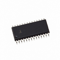
IC DAC 12-BIT 80MSPS 28-SOIC
Manufacturer
Intersil
Datasheet
1.HI5735KCBZ.pdf
(11 pages)
Specifications of HI5735KCB
Settling Time
20ns
Number Of Bits
12
Data Interface
Parallel
Number Of Converters
1
Voltage Supply Source
Analog and Digital, Dual ±
Power Dissipation (max)
650mW
Operating Temperature
0°C ~ 70°C
Mounting Type
Surface Mount
Package / Case
28-SOIC (7.5mm Width)
Lead Free Status / RoHS Status
Contains lead / RoHS non-compliant
Available stocks
Company
Part Number
Manufacturer
Quantity
Price

Part Number:
HI5735KCB
Manufacturer:
INTERSIL
Quantity:
20 000
Company:
Part Number:
HI5735KCBZ
Manufacturer:
MAXIM
Quantity:
1 001


Absolute Maximum Ratings
Digital Supply Voltage V
Negative Digital Supply Voltage DV
Negative Analog Supply Voltage AV
Digital Input Voltages (D11-D0, CLK) to DGND. . . . . DV
Internal Reference Output Current. . . . . . . . . . . . . . . . . . . . ±2.5mA
Voltage from CTRL IN to AV
Control Amplifier Output Current . . . . . . . . . . . . . . . . . . . . . ±2.5mA
Reference Input Voltage Range . . . . . . . . . . . . . . . . . .-3.7V to AV
Analog Output Current (I
Operating Conditions
Temperature Range
CAUTION: Stresses above those listed in “Absolute Maximum Ratings” may cause permanent damage to the device. This is a stress only rating and operation of the
device at these or any other conditions above those indicated in the operational sections of this specification is not implied.
NOTE:
Electrical Specifications
SYSTEM PERFORMANCE
Resolution
Integral Linearity Error, INL
Differential Linearity Error, DNL
Offset Error, I
Full Scale Gain Error, FSE
Offset Drift Coefficient
Full Scale Output Current, I
Output Voltage Compliance Range
DYNAMIC CHARACTERISTICS
Throughput Rate
Output Voltage Full Scale Step
Settling Time, t
Single Glitch Area, GE (Peak)
Doublet Glitch Area, (Net)
Output Slew Rate
Output Rise Time
Output Fall Time
Differential Gain
Differential Phase
Spurious Free Dynamic Range to Nyquist
(Note 3)
1. θ
HI5735KCB . . . . . . . . . . . . . . . . . . . . . . . . . . . . . . . . 0
JA
is measured with the component mounted on an evaluation PC board in free air.
OS
SETT
PARAMETER
Full Scale
CC
OUT
to DGND . . . . . . . . . . . . . . . . . . . +5.5V
EE
FS
) . . . . . . . . . . . . . . . . . . . . . . . . . 30mA
. . . . . . . . . . . . . . . . . . . . 2.5V to 0V
3
EE
EE
AV
to DGND . . . . . . . . . . -5.5V
EE
to AGND, ARTN . . . . . -5.5V
, DV
EE
= -4.94 to -5.46V, V
(Note 4) (“Best Fit” Straight Line)
(Note 4)
(Note 4)
(Notes 2, 4)
(Note 3)
(Note 3)
(Note 5)
To ±0.5 LSB Error Band R
(Note 3)
R
R
(Note 3)
R
(Note 3)
R
(Note 3)
R
R
f
f
CLK
CLK
L
L
L
L
L
L
CC
o
C to 70
= 50Ω (Note 3)
= 50Ω, DAC Operating in Latched Mode
= 50Ω, DAC Operating in Latched Mode
= 50Ω, DAC Operating in Latched Mode
= 50Ω (Note 3)
= 50Ω (Note 3)
= 40MHz, f
= 80MHz, f
to -0.5V
EE
o
C
HI5735
CC
TEST CONDITIONS
OUT
OUT
= +4.75 to +5.25V, V
= 2.02MHz, 20MHz Span
= 2.02MHz, 40MHz Span
Thermal Information
Thermal Resistance (Typical, Note 1)
Maximum Junction Temperature
Maximum Storage Temperature Range . . . . . . . . . . -65
Maximum Lead Temperature (Soldering 10s) . . . . . . . . . . . . .300
Plastic Packages . . . . . . . . . . . . . . . . . . . . . . . . . . . . . . . . .150
(SOIC - Lead Tips Only)
L
SOIC Package . . . . . . . . . . . . . . . . . . . . . . . . . . .
= 50Ω
REF
= Internal T
A
-1.25
= 25
MIN
12
80
-
-
-
-
-
-
-
-
-
-
-
-
-
-
-
-
o
C for All Typical Values
20.48
1,000
TYP
0.75
0.15
0.07
675
470
0.5
20
20
70
70
1
5
3
-
-
-
-
MAX
0.05
1.5
1.0
75
10
0
-
-
-
-
-
-
-
-
-
-
-
-
-
o
θ
C to 150
JA
UNITS
µA/
MSPS
pV-s
pV-s
V/µs
LSB
LSB
Deg
(
Bits
dBc
dBc
75
mA
µA
o
ns
ps
ps
%
%
V
C/W)
o
C
o
o
o
C
C
C
Related parts for HI5735KCB
Image
Part Number
Description
Manufacturer
Datasheet
Request
R

Part Number:
Description:
12-bit, 80 Msps, High Speed Video D/a Converter
Manufacturer:
Intersil Corporation
Datasheet:
Part Number:
Description:
Intersil Corporation [CMOS Serial Controller Interface]
Manufacturer:
Intersil Corporation
Datasheet:
Part Number:
Description:
Manufacturer:
Intersil Corporation
Datasheet:
Part Number:
Description:
357-036-542-201 CARDEDGE 36POS DL .156 BLK LOPRO
Manufacturer:
Intersil Corporation
Datasheet:
Part Number:
Description:
1024-Word x 4-Bit LSI Static RAM
Manufacturer:
Intersil Corporation
Datasheet:
Part Number:
Description:
General Purpose NPN Transistor Arrays FN341.4
Manufacturer:
Intersil Corporation
Datasheet:
Part Number:
Description:
CMOS 16-Bit Microprocessor
Manufacturer:
Intersil Corporation
Datasheet:
Part Number:
Description:
Manufacturer:
Intersil Corporation
Datasheet:
Part Number:
Description:
Manufacturer:
Intersil Corporation
Datasheet:
Part Number:
Description:
Manufacturer:
Intersil Corporation
Datasheet:
Part Number:
Description:
Manufacturer:
Intersil Corporation
Datasheet:
Part Number:
Description:
CMOS 6-Bit Latch and Decoder Memory Interfaces
Manufacturer:
Intersil Corporation
Datasheet:
Part Number:
Description:
CA3046General Purpose NPN Transistor Arrays
Manufacturer:
Intersil Corporation
Datasheet:
Part Number:
Description:
Manufacturer:
Intersil Corporation
Datasheet:
Part Number:
Description:
TR909 DLC/FLC SLIC with Low Power Standby
Manufacturer:
Intersil Corporation
Datasheet: