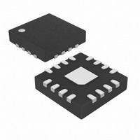
MAX5548ETE+T Maxim Integrated Products, MAX5548ETE+T Datasheet - Page 4

MAX5548ETE+T
Manufacturer Part Number
MAX5548ETE+T
Description
IC DAC 8BIT DUAL 30MA 16-TQFN
Manufacturer
Maxim Integrated Products
Datasheet
1.MAX5548ETE.pdf
(15 pages)
Specifications of MAX5548ETE+T
Settling Time
30µs
Number Of Bits
8
Data Interface
Serial
Number Of Converters
2
Voltage Supply Source
Single Supply
Operating Temperature
-40°C ~ 85°C
Mounting Type
Surface Mount
Package / Case
16-TQFN Exposed Pad
Lead Free Status / RoHS Status
Lead free / RoHS Compliant
Power Dissipation (max)
-
Dual, 8-Bit, Programmable, 30mA
High-Output-Current DAC
ELECTRICAL CHARACTERISTICS (continued)
(V
V
4
Note 1: 100% production tested at T
Note 2: INL linearity is guaranteed from code 15 to code 255.
Note 3: Connect a resistor from FSADJ_ to GND to adjust the full-scale current. See the Reference Architecture and Operation section.
Note 4: Settling time is measured from (0.25 x full scale) to (0.75 x full scale).
Note 5: The device draws higher supply current when the digital inputs are driven with voltages between (V
Setup Time for STOP Condition
Maximum Capacitive Load for
Each Bus Line
SPI TIMING CHARACTERISTICS (Figure 6)
SCLK Clock Period
SCLK Pulse-Width High
SCLK Pulse-Width Low
CS Fall to SCLK Rise Setup Time
SCLK Rise to CS Rise Hold Time
DIN Setup Time
DIN Hold Time
SCLK Fall to DOUT Transition
CS Fall to DOUT Enable
CS Rise to DOUT Disable
SCLK Rise to CS Fall Delay
CS Rise to SCLK Rise Hold Time
CS Pulse-Width High
SPI TIMING CHARACTERISTICS FOR DAISY CHAINING (Figure 6)
SCLK Clock Period
SCLK Pulse-Width High
SCLK Pulse-Width Low
CS Fall to SCLK Rise Setup Time
SCLK Rise to CS Rise Hold Time
DIN Setup Time
DIN Hold Time
SCLK Fall to DOUT Transition
CS Fall to DOUT Enable
CS Rise to DOUT Disable
SCLK Rise to CS Fall Delay
CS Rise to SCLK Rise Hold Time
CS Pulse-Width High
SCLK/SCL
DD
_______________________________________________________________________________________
= +2.7V to +5.25V, GND = 0, V
0.5V). See the Supply Current vs. Digital Input Voltage graph in the Typical Operating Characteristics.
PARAMETER
= 0, T
A
= -40°C to +85°C, unless otherwise noted. Typical values are at V
A
SYMBOL
t
= +25°C. Limits over temperature are guaranteed by design.
SU:STO
REFIN
t
t
t
t
t
t
t
t
t
t
t
t
t
t
t
t
CSW
CSW
t
t
t
t
t
t
CSS
CSH
t
DO1
CSE
CSD
t
t
CSS
CSH
t
DO1
CSE
CSD
C
CS0
CS1
CS0
CS1
CH
DH
CH
DH
CP
CL
DS
CP
CL
DS
B
= +1.25V, internal reference, R
C
C
C
C
C
C
LOAD
LOAD
LOAD
LOAD
LOAD
LOAD
= 30pF
= 30pF
= 30pF
= 30pF
= 30pF
= 30pF
CONDITIONS
FSADJ_
DD
= 20kΩ; compliance voltage = (V
= +3.0V and T
MIN
160
100
100
200
100
40
40
25
50
40
50
40
80
80
25
50
40
50
40
0
0
A
= +25°C.) (Note 1)
TYP
400
DD
- 0.5V) and (GND +
MAX
40
40
40
40
40
40
DD
UNITS
- 0.6V),
pF
ns
ns
ns
ns
ns
ns
ns
ns
ns
ns
ns
ns
ns
ns
ns
ns
ns
ns
ns
ns
ns
ns
ns
ns
ns
ns
ns


