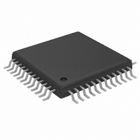
MAX5856AECM+D Maxim Integrated Products, MAX5856AECM+D Datasheet - Page 13

MAX5856AECM+D
Manufacturer Part Number
MAX5856AECM+D
Description
IC DAC 8BIT DUAL 300MSPS 48-TQFP
Manufacturer
Maxim Integrated Products
Datasheet
1.MAX5856AECMD.pdf
(23 pages)
Specifications of MAX5856AECM+D
Settling Time
11ns
Number Of Bits
8
Data Interface
Parallel
Number Of Converters
2
Voltage Supply Source
Single Supply
Power Dissipation (max)
792mW
Operating Temperature
-40°C ~ 85°C
Mounting Type
Surface Mount
Package / Case
48-TQFP Exposed Pad, 48-eTQFP, 48-HTQFP, 48-VQFP
Lead Free Status / RoHS Status
Lead free / RoHS Compliant
The MAX5856A dual, high-speed, 8-bit, current-output
DAC provides superior performance in communication
systems requiring low-distortion analog-signal recon-
struction. The MAX5856A combines two DAC cores with
4x/2x/1x programmable digital interpolation filters, a PLL
clock multiplier, divide-by-N clock output, and an on-
chip 1.24V reference. The DAC current outputs can be
configured for differential or single-ended operation. The
full-scale output current range is adjustable from 2mA to
20mA to optimize power dissipation and gain control.
The MAX5856A accepts an input data rate up to
165MHz or a DAC conversion rate up to 300MHz. The
inputs are latched on the rising edge of the clock. The
outputs are latched on the following rising edge.
The two-stage digital interpolation filters are program-
mable to 4x, 2x, or no interpolation. When operating in
4x interpolation mode, the interpolator increases the
DAC conversion rate by a factor of four, providing a
four-fold increase in separation between the recon-
structed waveform spectrum and its first image.
The on-chip PLL clock multiplier generates and distrib-
utes all internal, synchronized high-speed clock signals
required by the input data latches, interpolation filters,
and DAC cores. The on-chip PLL includes phase
detector, VCO, prescalar, and charge pump circuits.
The PLL can be enabled or disabled through PLLEN.
______________________________________________________________________________________
DA7–DA0
DB7–DB0
CW
IDE
Dual 8-Bit, 300Msps DAC with 4x/2x/1x
Detailed Description
MAX5856A
8
8
DV
DD
REGISTER
REGISTER
INPUT
INPUT
DGND
PV
DD
CONTROL REGISTER
AV
8
8
DD
F1EN
INTERPOLATION
INTERPOLATION
PGND
2x DIGITAL
2x DIGITAL
Interpolation Filters and PLL
FILTER
FILTER
8
8
REFO
1.2V REFERENCE AND CONTROL AMPLIFIER
INTERPOLATION
INTERPOLATION
F2EN
The analog and digital sections of the MAX5856A have
separate power supply inputs (AV
a separate supply input is provided for the PLL clock
multiplier (PV
a 2.7V to 3.3V single supply.
The MAX5856A features three power modes: normal,
standby, and power-down. These modes allow efficient
power management. In power-down, the MAX5856A
consumes only 1µA of supply current. Wake-up time
from standby mode to normal DAC operation is 0.7µs.
An 8-bit control word routed through channel A’s data
port programs the gain matching, interpolator configu-
ration, and operational mode of the MAX5856A. The
control word is latched on the falling edge of control-
word write pulse (CW). The CW signal is asynchronous
with CLK and CLKXN/CLKXP; therefore, the conversion
clock (CLK or CLKXN/CLKXP) can run uninterrupted
when a control word is written to the device.
Table 1 illustrates the control word format and function.
The gain on channel A can be adjusted to achieve gain
matching between two channels in a user’s system.
The gain on channel A can be adjusted from +0.4dB to
-0.35dB in steps of 0.05dB by using bits G3 to G0 (see
Table 3).
2x DIGITAL
2x DIGITAL
FILTER
FILTER
REN
CLKXP
PLL CLOCK MULTIPLIER
8
8
CLKXN
DD
REFR
300MHz
300MHz
). AV
8-BIT
8-BIT
DAC
DAC
CLK
R
SET
DD
, DV
Functional Diagram
AGND
Programming the DAC
DD
OUTPA
OUTNA
OUTPB
OUTNB
, and PV
LOCK
PLLEN
DD
PLLF
and DV
DD
operate from
DD
). Also,
13


