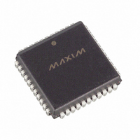
MAX547BEQH+D Maxim Integrated Products, MAX547BEQH+D Datasheet - Page 10

MAX547BEQH+D
Manufacturer Part Number
MAX547BEQH+D
Description
IC DAC 13BIT OCTAL PAR 44-PLCC
Manufacturer
Maxim Integrated Products
Datasheet
1.MAX547BCQH-D.pdf
(16 pages)
Specifications of MAX547BEQH+D
Settling Time
5µs
Number Of Bits
13
Data Interface
Parallel
Number Of Converters
8
Voltage Supply Source
Dual ±
Power Dissipation (max)
1.07W
Operating Temperature
-40°C ~ 85°C
Mounting Type
Surface Mount
Package / Case
44-LCC, 44-PLCC
Lead Free Status / RoHS Status
Lead free / RoHS Compliant
For positive unipolar output operation, set AGND_ to
(REF_/2). For example, if you use Figure 4’s circuit with,
a 4.096V reference and offset AGND_ by 2.048V with
matched resistors (R1 = R2) and an op amp, it results in
a 0V to 4.0955V (nominal) unipolar output voltage,
where 1LSB = 500µV. In general, the maximum current
flowing out of any AGND_ pin is given by:
Octal, 13-Bit Voltage-Output
DAC with Parallel Interface
Table 3. MAX547 Bipolar Code Table
10
Figure 4. Offsetting AGND –
REF
I
AGND_
______________________________________________________________________________________
1 1111 1111 1111
1 0000 0000 0001
1 0000 0000 0000
0 1111 1111 1111
0 0000 0000 0001
0 0000 0000 0000
DIGITAL INPUTS NOT SHOWN.
NOT ALL DACS SHOWN.
R1
R2
INPUT
(AGND_ = 0V)
Positive Unipolar Output Voltage Range
REF_
1 F
AGNDAB
5k
REFAB
AGND_
1 F
1 F
DAC A
DAC B
V
V
DD
SS
+REF_
+REF_
-REF_
-REF_
MAX547
+5V
-5V
(AGND_ = REF_/2)
OUTPUT
V
V
-REF_
DD
SS
0V
(
(
(
(
———
———
———
———
1 F
4095
4096
4096
4096
4095
4096
1 F
1
1
)
)
)
)
VOUTA
VOUTB
The AGND_ inputs can be offset by any voltage within the
supply rails if the voltage at the referring REF_ input is
higher than the voltage at the AGND_ input. Select the
reference voltage and the voltage at AGND_ so the
resulting output voltages do not come within ±0.6V of the
supply rails. Figure 4’s circuit shows one way to add posi-
tive offset to AGND_; make sure that the op amp used
has sufficient current-sink capability to take up the
remaining AGND_ current:
Another way is to digitally offset AGND_ by connecting
the output of one DAC to one or more AGND_ inputs. Do
not connect a DAC output to its own AGND_ input.
Table 5 summarizes the relationship between the refer-
ence and AGND_ potentials and the output voltage in
the different modes of operation.
The sequence in which the supply voltages come up is
not critical. However, we recommend that on power-up,
V
voltages. If you use other sequences, limit the current
into any reference pin to 10mA. Also, make sure that
V
a risk that this can occur at power-up, connect a
Schottky diode between V
Figure 5. We recommend that you not power up the
logic input pins before establishing the supply volt-
ages. If this is not possible and the digital lines can
drive more than 10mA, you should place current-limit-
ing resistors (e.g., 470Ω) in series with the logic pins.
If you want a ±2.5V full-scale output voltage swing, you
can use the MAX873 reference. It operates from a sin-
gle 5V supply and is specified to drive up to 10mA.
Therefore, it can drive all four reference inputs simulta-
neously. Because the maximum load impedance can
vary from 1.25kΩ to 12.5kΩ (four reference inputs in
parallel), the reference load current ranges from 2mA to
0.2mA (1.8mA maximum load step). The MAX873’s
Table 4. MAX547 Positive Unipolar Code Table
SS
SS
I
AGND_
comes up first, V
is never more than 300mV above ground. If there is
1 1111 1111 1111
1 0000 0000 0000
0 0000 0000 0000
(AGND_ = REF _ )
INPUT
REF_
Customizing the Output Voltage Range
5k
DD
Power-Supply Sequencing
AGND_
2
next, followed by the reference
SS
Reference Selection
and GND, as shown in
+REF_
OUTPUT
+REF – /2
0V
(
———
8191
8192
)


