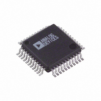
AD7835AS Analog Devices Inc, AD7835AS Datasheet - Page 16

AD7835AS
Manufacturer Part Number
AD7835AS
Description
IC DAC 14BIT QUAD PARA 44-MQFP
Manufacturer
Analog Devices Inc
Datasheet
1.AD7835ASZ.pdf
(28 pages)
Specifications of AD7835AS
Rohs Status
RoHS non-compliant
Settling Time
10µs
Number Of Bits
14
Data Interface
Parallel
Number Of Converters
4
Voltage Supply Source
Analog and Digital, Dual ±
Power Dissipation (max)
465mW
Operating Temperature
-40°C ~ 85°C
Mounting Type
Surface Mount
Package / Case
44-MQFP, 44-PQFP
Available stocks
Company
Part Number
Manufacturer
Quantity
Price
Company:
Part Number:
AD7835AS
Manufacturer:
AD
Quantity:
13 888
Company:
Part Number:
AD7835ASZ
Manufacturer:
OKI
Quantity:
490
Company:
Part Number:
AD7835ASZ
Manufacturer:
ADI
Quantity:
850
Company:
Part Number:
AD7835ASZ
Manufacturer:
Analog Devices Inc
Quantity:
10 000
Part Number:
AD7835ASZ
Manufacturer:
ADI/亚德诺
Quantity:
20 000
Company:
Part Number:
AD7835ASZ-REEL
Manufacturer:
Analog Devices Inc
Quantity:
10 000
AD7834/AD7835
BIPOLAR CONFIGURATION
100kΩ
Figure 20 shows the AD7834/AD7835 setup for ±5 V operation.
The
fed to the V
The code table for bipolar operation of the AD7834/AD7835 is
shown in Table 13.
Table 13. Code Table for Bipolar Operation
MSB
11
10
10
01
00
00
1
2
Binary Number in DAC Latch
V
For V
REF
R2
1
= V
AD588
ADDITIONAL PINS OMITTED FOR CLARITY
REF
100kΩ
REF
(+) = +5 V and V
1111
0000
0000
1111
0000
0000
R3
(+) – V
1μF
C1
REF
provides precision ±5 V tracking outputs that are
REF
(+) and V
10
11
5
7
9
(−).
1111
0000
0000
1111
0000
0000
12
Figure 20. Bipolar ±5 V Operation
AD588
REF
4
8
(−) = –5 V, 1 LSB = 10 V/2
13
REF
6
LSB
1111
0001
0000
1111
0001
0000
R1
39kΩ
(−) inputs of the AD7834/AD7835.
14
15
16
2
3
1
Analog Output (V
V
V
V
V
V
V
REF
REF
REF
REF
REF
REF
V
V
REF
REF
(−) + V
(−) + V
(−) + V
(−) + V
(−) + V
(−) V
+15V
V
DD
(+)
(–)
AD7834/
AD7835
–15V
V
SS
14
REF
REF
REF
REF
REF
+5V
V
= 10 V/16384 = 610 μV.
AGND
DGND
CC
1
V
1, 2
(16383/16384) V
(8193/16384) V
(8192/16384) V
(8191/16384) V
(1/16384) V
OUT
SIGNAL
OUT
GND
V
(–5V TO +5V)
)
OUT
Rev. D | Page 16 of 28
In Figure 20, full-scale and bipolar zero adjustments are
provided by varying the gain and balance on the AD588. R2
varies the gain on the AD588 while R3 adjusts the offset of both
the +5 V and –5 V outputs together with respect to ground.
For bipolar-zero adjustment, the DAC is loaded with
1000 . . . 0000 and R3 is adjusted until V
is adjusted by loading the DAC with all 1s and adjusting R2
until V
When bipolar zero and full-scale adjustment are not needed, R2
and R3 are omitted. Pin 12 on the AD588 should be connected to
Pin 11, and Pin 5 should be left floating.
OUT
= 5(8191/8192) V = 4.99939 V.
OUT
= 0 V. Full scale


