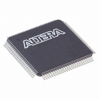
EPM570T100C3N Altera, EPM570T100C3N Datasheet - Page 74

EPM570T100C3N
Manufacturer Part Number
EPM570T100C3N
Description
IC MAX II CPLD 570 LE 100-TQFP
Manufacturer
Altera
Series
MAX® IIr
Specifications of EPM570T100C3N
Programmable Type
In System Programmable
Delay Time Tpd(1) Max
5.4ns
Voltage Supply - Internal
2.5V, 3.3V
Number Of Logic Elements/blocks
570
Number Of Macrocells
440
Number Of I /o
76
Operating Temperature
0°C ~ 85°C
Mounting Type
Surface Mount
Package / Case
100-TQFP, 100-VQFP
Voltage
2.5V, 3.3V
Memory Type
FLASH
Number Of Logic Elements/cells
570
Family Name
MAX II
# Macrocells
440
Frequency (max)
3.01205GHz
Propagation Delay Time
5.4ns
Number Of Logic Blocks/elements
57
# I/os (max)
76
Operating Supply Voltage (typ)
2.5/3.3V
In System Programmable
Yes
Operating Supply Voltage (min)
2.375V
Operating Supply Voltage (max)
3.6V
Operating Temp Range
0C to 85C
Operating Temperature Classification
Commercial
Mounting
Surface Mount
Pin Count
100
Package Type
TQFP
Lead Free Status / RoHS Status
Lead free / RoHS Compliant
Features
-
Lead Free Status / Rohs Status
Compliant
Other names
544-1315
EPM570T100C3N
EPM570T100C3N
Available stocks
Company
Part Number
Manufacturer
Quantity
Price
Part Number:
EPM570T100C3N
Manufacturer:
ALTERA/阿尔特拉
Quantity:
20 000
5–16
Table 5–21. UFM Block Internal Timing Microparameters (Part 3 of 3)
Figure 5–3. UFM Read Waveforms
MAX II Device Handbook
t
t
t
t
Symbol
OE
RA
OSC S
OSC H
Delay from data
register clock to data
register output
Maximum read
access time
Maximum delay
between the
OSC_ENA rising
edge to the
erase/program signal
rising edge
Minimum delay
allowed from the
erase/program signal
going low to
OSC_ENA signal
going low
Parameter
OSC_ENA
Program
DRDout
DRShft
ARShft
DRDin
ARClk
ARDin
DRClk
Erase
Figure 5–3
UFM block timing parameters shown in
Busy
t
t
ASU
ADS
through
Min
180
250
250
–3 Speed
—
Grade
t
ACLK
Max
—
65
—
—
9 Address Bits
Figure 5–5
MAX II / MAX IIG
Min
180
250
250
–4 Speed
—
Grade
Max
—
65
—
—
t
t
ADH
show the read, program, and erase waveforms for
AH
t
DCO
t
DSS
Min
180
250
250
–5 Speed
—
Grade
t
DCLK
Table
Max
—
65
—
—
16 Data Bits
5–21.
Min Max Min Max Min Max
180
250
250
–6 Speed
—
Grade
Chapter 5: DC and Switching Characteristics
—
65
—
—
t
DSH
180
250
250
–7 Speed
—
MAX IIZ
© August 2009 Altera Corporation
Grade
Timing Model and Specifications
—
65
—
—
180
250
250
–8 Speed
—
Grade
—
65
—
—
Unit
ns
ns
ns
ns


