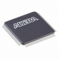
EPM570T100C3N Altera, EPM570T100C3N Datasheet - Page 84

EPM570T100C3N
Manufacturer Part Number
EPM570T100C3N
Description
IC MAX II CPLD 570 LE 100-TQFP
Manufacturer
Altera
Series
MAX® IIr
Specifications of EPM570T100C3N
Programmable Type
In System Programmable
Delay Time Tpd(1) Max
5.4ns
Voltage Supply - Internal
2.5V, 3.3V
Number Of Logic Elements/blocks
570
Number Of Macrocells
440
Number Of I /o
76
Operating Temperature
0°C ~ 85°C
Mounting Type
Surface Mount
Package / Case
100-TQFP, 100-VQFP
Voltage
2.5V, 3.3V
Memory Type
FLASH
Number Of Logic Elements/cells
570
Family Name
MAX II
# Macrocells
440
Frequency (max)
3.01205GHz
Propagation Delay Time
5.4ns
Number Of Logic Blocks/elements
57
# I/os (max)
76
Operating Supply Voltage (typ)
2.5/3.3V
In System Programmable
Yes
Operating Supply Voltage (min)
2.375V
Operating Supply Voltage (max)
3.6V
Operating Temp Range
0C to 85C
Operating Temperature Classification
Commercial
Mounting
Surface Mount
Pin Count
100
Package Type
TQFP
Lead Free Status / RoHS Status
Lead free / RoHS Compliant
Features
-
Lead Free Status / Rohs Status
Compliant
Other names
544-1315
EPM570T100C3N
EPM570T100C3N
Available stocks
Company
Part Number
Manufacturer
Quantity
Price
Part Number:
EPM570T100C3N
Manufacturer:
ALTERA/阿尔特拉
Quantity:
20 000
5–26
Table 5–34. MAX II JTAG Timing Parameters (Part 2 of 2)
Referenced Documents
MAX II Device Handbook
t
t
t
t
t
t
t
t
t
t
Notes to
(1) Minimum clock period specified for 10 pF load on the TDO pin. Larger loads on TDO will degrade the maximum TCK
(2) This specification is shown for 3.3-V LVTTL/LVCMOS and 2.5-V LVTTL/LVCMOS operation of the JTAG pins. For 1.8-V
JP SU
JP H
JP CO
JP ZX
JP XZ
JS SU
JS H
JS CO
JS ZX
JS XZ
frequency.
LVTTL/LVCMOS and 1.5-V LVCMOS, the t
Symbol
Table
5–34:
JTAG port setup time
JTAG port hold time
JTAG port clock to output
JTAG port high impedance to valid output
JTAG port valid output to high impedance
Capture register setup time
Capture register hold time
Update register clock to output
Update register high impedance to valid output
Update register valid output to high impedance
This chapter references the following documents:
■
■
■
■
■
■
■
I/O Structure section in the
Handbook
Hot Socketing and Power-On Reset in MAX II Devices
Handbook
Operating Requirements for Altera Devices Data Sheet
PowerPlay Power Analysis
Understanding and Evaluating Power in MAX II Devices
Handbook
Understanding Timing in MAX II Devices
Using MAX II Devices in Multi-Voltage Systems
Handbook
Parameter
JPS U
(2)
minimum is 6 ns and t
(2)
chapter in volume 3 of the Quartus II Handbook
MAX II Architecture
J PC O
(2)
(2)
, t
JP ZX
, and t
Min
10
—
—
—
10
—
—
—
8
8
JP XZ
chapter in the MAX II Device Handbook
are maximum values at 35 ns.
chapter in the MAX II Device
chapter in the MAX II Device
Chapter 5: DC and Switching Characteristics
Max
—
—
15
15
15
—
—
25
25
25
chapter in the MAX II Device
chapter in the MAX II Device
© August 2009 Altera Corporation
Unit
ns
ns
ns
ns
ns
ns
ns
ns
ns
ns
Referenced Documents


