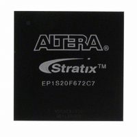
EP1S20F672C7 Altera, EP1S20F672C7 Datasheet - Page 228

EP1S20F672C7
Manufacturer Part Number
EP1S20F672C7
Description
IC STRATIX FPGA 20K LE 672-FBGA
Manufacturer
Altera
Series
Stratix®r
Datasheet
1.EP1S10F780C7.pdf
(276 pages)
Specifications of EP1S20F672C7
Number Of Logic Elements/cells
18460
Number Of Labs/clbs
1846
Total Ram Bits
1669248
Number Of I /o
426
Voltage - Supply
1.425 V ~ 1.575 V
Mounting Type
Surface Mount
Operating Temperature
0°C ~ 85°C
Package / Case
672-FBGA
Family Name
Stratix
Number Of Logic Blocks/elements
18460
# I/os (max)
426
Frequency (max)
420.17MHz
Process Technology
0.13um (CMOS)
Operating Supply Voltage (typ)
1.5V
Logic Cells
18460
Ram Bits
1669248
Operating Supply Voltage (min)
1.425V
Operating Supply Voltage (max)
1.575V
Operating Temp Range
0C to 85C
Operating Temperature Classification
Commercial
Mounting
Surface Mount
Pin Count
672
Package Type
FBGA
Lead Free Status / RoHS Status
Contains lead / RoHS non-compliant
Number Of Gates
-
Lead Free Status / Rohs Status
Not Compliant
Other names
544-1113
Available stocks
Company
Part Number
Manufacturer
Quantity
Price
Company:
Part Number:
EP1S20F672C7
Manufacturer:
SHARP
Quantity:
3 509
Company:
Part Number:
EP1S20F672C7
Manufacturer:
ALTERA
Quantity:
528
Part Number:
EP1S20F672C7
Manufacturer:
ALTERA/阿尔特拉
Quantity:
20 000
Company:
Part Number:
EP1S20F672C7N
Manufacturer:
Harting
Quantity:
1 000
Company:
Part Number:
EP1S20F672C7N
Manufacturer:
ALTERA
Quantity:
3 000
Timing Model
4–58
Stratix Device Handbook, Volume 1
Figure 4–6
different I/O banks.
Figure 4–6. I/O Skew Across Two I/O Banks
Table 4–97
horizontal I/O pins (side banks 1, 2, 5, 6) and vertical I/O pins (top and
bottom banks 3, 4, 7, 8). The timing parameters define the skew within an
I/O bank, across two neighboring I/O banks on the same side of the
device, across all horizontal I/O banks, across all vertical I/O banks, and
the skew for the overall device.
t
t
t
t
SB_HIO
SB_VIO
SS_HIO
SS_VIO
Table 4–97. Output Pin Timing Skew Definitions (Part 1 of 2)
Symbol
shows the case where four IOE registers are located in two
defines the timing parameters used to define the timing for
I/O Pin A
I/O Pin B
I/O Pin C
I/O Pin D
Row I/O (HIO) within one I/O bank
Column I/O (VIO) within one I/O bank
Row I/O (HIO) same side of the device, across two
banks
Column I/O (VIO) same side of the device, across two
banks
I/O Pin Skew across
(2)
(2)
Common Source of GCLK
I/O Bank
I/O Bank
two Banks
Definition
(1)
Altera Corporation
I/O Pin A
I/O Pin C
I/O Pin B
I/O Pin D
(1)
January 2006


