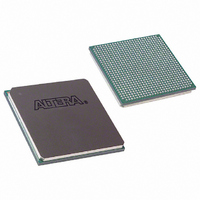
EP1S25F780C7N Altera, EP1S25F780C7N Datasheet - Page 15

EP1S25F780C7N
Manufacturer Part Number
EP1S25F780C7N
Description
IC STRATIX FPGA 25K LE 780-FBGA
Manufacturer
Altera
Series
Stratix®r
Datasheet
1.EP1S10F780C7.pdf
(276 pages)
Specifications of EP1S25F780C7N
Number Of Logic Elements/cells
25660
Number Of Labs/clbs
2566
Total Ram Bits
1944576
Number Of I /o
597
Voltage - Supply
1.425 V ~ 1.575 V
Mounting Type
Surface Mount
Operating Temperature
0°C ~ 85°C
Package / Case
780-FBGA
Family Name
Stratix
Number Of Logic Blocks/elements
25660
# I/os (max)
597
Frequency (max)
420.17MHz
Process Technology
0.13um (CMOS)
Operating Supply Voltage (typ)
1.5V
Logic Cells
25660
Ram Bits
1944576
Operating Supply Voltage (min)
1.425V
Operating Supply Voltage (max)
1.575V
Operating Temp Range
0C to 85C
Operating Temperature Classification
Commercial
Mounting
Surface Mount
Pin Count
780
Package Type
FC-FBGA
Lead Free Status / RoHS Status
Lead free / RoHS Compliant
Number Of Gates
-
Lead Free Status / Rohs Status
Compliant
Other names
544-1860
EP1S25F780C7N
EP1S25F780C7N
Available stocks
Company
Part Number
Manufacturer
Quantity
Price
Company:
Part Number:
EP1S25F780C7N
Manufacturer:
ALTERA
Quantity:
648
Part Number:
EP1S25F780C7N
Manufacturer:
ALTERA/阿尔特拉
Quantity:
20 000
- Current page: 15 of 276
- Download datasheet (4Mb)
Functional
Description
Altera Corporation
July 2005
S51002-3.2
Stratix
architecture to implement custom logic. A series of column and row
interconnects of varying length and speed provide signal interconnects
between logic array blocks (LABs), memory block structures, and DSP
blocks.
The logic array consists of LABs, with 10 logic elements (LEs) in each
LAB. An LE is a small unit of logic providing efficient implementation of
user logic functions. LABs are grouped into rows and columns across the
device.
M512 RAM blocks are simple dual-port memory blocks with 512 bits plus
parity (576 bits). These blocks provide dedicated simple dual-port or
single-port memory up to 18-bits wide at up to 318 MHz. M512 blocks are
grouped into columns across the device in between certain LABs.
M4K RAM blocks are true dual-port memory blocks with 4K bits plus
parity (4,608 bits). These blocks provide dedicated true dual-port, simple
dual-port, or single-port memory up to 36-bits wide at up to 291 MHz.
These blocks are grouped into columns across the device in between
certain LABs.
M-RAM blocks are true dual-port memory blocks with 512K bits plus
parity (589,824 bits). These blocks provide dedicated true dual-port,
simple dual-port, or single-port memory up to 144-bits wide at up to
269 MHz. Several M-RAM blocks are located individually or in pairs
within the device’s logic array.
Digital signal processing (DSP) blocks can implement up to either eight
full-precision 9 × 9-bit multipliers, four full-precision 18 × 18-bit
multipliers, or one full-precision 36 × 36-bit multiplier with add or
subtract features. These blocks also contain 18-bit input shift registers for
digital signal processing applications, including FIR and infinite impulse
response (IIR) filters. DSP blocks are grouped into two columns in each
device.
Each Stratix device I/O pin is fed by an I/O element (IOE) located at the
end of LAB rows and columns around the periphery of the device. I/O
pins support numerous single-ended and differential I/O standards.
Each IOE contains a bidirectional I/O buffer and six registers for
registering input, output, and output-enable signals. When used with
®
devices contain a two-dimensional row- and column-based
2. Stratix Architecture
2–1
Related parts for EP1S25F780C7N
Image
Part Number
Description
Manufacturer
Datasheet
Request
R

Part Number:
Description:
CYCLONE II STARTER KIT EP2C20N
Manufacturer:
Altera
Datasheet:

Part Number:
Description:
CPLD, EP610 Family, ECMOS Process, 300 Gates, 16 Macro Cells, 16 Reg., 16 User I/Os, 5V Supply, 35 Speed Grade, 24DIP
Manufacturer:
Altera Corporation
Datasheet:

Part Number:
Description:
CPLD, EP610 Family, ECMOS Process, 300 Gates, 16 Macro Cells, 16 Reg., 16 User I/Os, 5V Supply, 15 Speed Grade, 24DIP
Manufacturer:
Altera Corporation
Datasheet:

Part Number:
Description:
Manufacturer:
Altera Corporation
Datasheet:

Part Number:
Description:
CPLD, EP610 Family, ECMOS Process, 300 Gates, 16 Macro Cells, 16 Reg., 16 User I/Os, 5V Supply, 30 Speed Grade, 24DIP
Manufacturer:
Altera Corporation
Datasheet:

Part Number:
Description:
High-performance, low-power erasable programmable logic devices with 8 macrocells, 10ns
Manufacturer:
Altera Corporation
Datasheet:

Part Number:
Description:
High-performance, low-power erasable programmable logic devices with 8 macrocells, 7ns
Manufacturer:
Altera Corporation
Datasheet:

Part Number:
Description:
Classic EPLD
Manufacturer:
Altera Corporation
Datasheet:

Part Number:
Description:
High-performance, low-power erasable programmable logic devices with 8 macrocells, 10ns
Manufacturer:
Altera Corporation
Datasheet:

Part Number:
Description:
Manufacturer:
Altera Corporation
Datasheet:

Part Number:
Description:
Manufacturer:
Altera Corporation
Datasheet:

Part Number:
Description:
Manufacturer:
Altera Corporation
Datasheet:

Part Number:
Description:
CPLD, EP610 Family, ECMOS Process, 300 Gates, 16 Macro Cells, 16 Reg., 16 User I/Os, 5V Supply, 25 Speed Grade, 24DIP
Manufacturer:
Altera Corporation
Datasheet:


