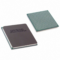
EP1S25F780C7N Altera, EP1S25F780C7N Datasheet - Page 41

EP1S25F780C7N
Manufacturer Part Number
EP1S25F780C7N
Description
IC STRATIX FPGA 25K LE 780-FBGA
Manufacturer
Altera
Series
Stratix®r
Datasheet
1.EP1S10F780C7.pdf
(276 pages)
Specifications of EP1S25F780C7N
Number Of Logic Elements/cells
25660
Number Of Labs/clbs
2566
Total Ram Bits
1944576
Number Of I /o
597
Voltage - Supply
1.425 V ~ 1.575 V
Mounting Type
Surface Mount
Operating Temperature
0°C ~ 85°C
Package / Case
780-FBGA
Family Name
Stratix
Number Of Logic Blocks/elements
25660
# I/os (max)
597
Frequency (max)
420.17MHz
Process Technology
0.13um (CMOS)
Operating Supply Voltage (typ)
1.5V
Logic Cells
25660
Ram Bits
1944576
Operating Supply Voltage (min)
1.425V
Operating Supply Voltage (max)
1.575V
Operating Temp Range
0C to 85C
Operating Temperature Classification
Commercial
Mounting
Surface Mount
Pin Count
780
Package Type
FC-FBGA
Lead Free Status / RoHS Status
Lead free / RoHS Compliant
Number Of Gates
-
Lead Free Status / Rohs Status
Compliant
Other names
544-1860
EP1S25F780C7N
EP1S25F780C7N
Available stocks
Company
Part Number
Manufacturer
Quantity
Price
Company:
Part Number:
EP1S25F780C7N
Manufacturer:
ALTERA
Quantity:
648
Part Number:
EP1S25F780C7N
Manufacturer:
ALTERA/阿尔特拉
Quantity:
20 000
- Current page: 41 of 276
- Download datasheet (4Mb)
Altera Corporation
July 2005
M512 RAM Block
The M512 RAM block is a simple dual-port memory block and is useful
for implementing small FIFO buffers, DSP, and clock domain transfer
applications. Each block contains 576 RAM bits (including parity bits).
M512 RAM blocks can be configured in the following modes:
■
■
■
■
■
When configured as RAM or ROM, you can use an initialization file to
pre-load the memory contents.
The memory address depths and output widths can be configured as
512 × 1, 256 × 2, 128 × 4, 64 × 8 (64 × 9 bits with parity), and 32 × 16
(32 × 18 bits with parity). Mixed-width configurations are also possible,
allowing different read and write widths.
possible M512 RAM block configurations.
When the M512 RAM block is configured as a shift register block, a shift
register of size up to 576 bits is possible.
The M512 RAM block can also be configured to support serializer and
deserializer applications. By using the mixed-width support in
combination with DDR I/O standards, the block can function as a
SERDES to support low-speed serial I/O standards using global or
regional clocks. See
dedicated SERDES in Stratix devices.
Read Port
Table 2–4. M512 RAM Block Configurations (Simple Dual-Port RAM)
512 × 1
256 × 2
128 × 4
32 × 16
32 × 18
64 × 8
64 × 9
Simple dual-port RAM
Single-port RAM
FIFO
ROM
Shift register
512 × 1
v
v
v
v
v
“I/O Structure” on page 2–104
256 × 2
v
v
v
v
v
128 × 4
v
v
v
v
Write Port
Stratix Device Handbook, Volume 1
64 × 8
v
v
v
Table 2–4
32 × 16
v
v
v
v
for details on
summarizes the
Stratix Architecture
64 × 9
v
32 × 18
v
2–27
Related parts for EP1S25F780C7N
Image
Part Number
Description
Manufacturer
Datasheet
Request
R

Part Number:
Description:
CYCLONE II STARTER KIT EP2C20N
Manufacturer:
Altera
Datasheet:

Part Number:
Description:
CPLD, EP610 Family, ECMOS Process, 300 Gates, 16 Macro Cells, 16 Reg., 16 User I/Os, 5V Supply, 35 Speed Grade, 24DIP
Manufacturer:
Altera Corporation
Datasheet:

Part Number:
Description:
CPLD, EP610 Family, ECMOS Process, 300 Gates, 16 Macro Cells, 16 Reg., 16 User I/Os, 5V Supply, 15 Speed Grade, 24DIP
Manufacturer:
Altera Corporation
Datasheet:

Part Number:
Description:
Manufacturer:
Altera Corporation
Datasheet:

Part Number:
Description:
CPLD, EP610 Family, ECMOS Process, 300 Gates, 16 Macro Cells, 16 Reg., 16 User I/Os, 5V Supply, 30 Speed Grade, 24DIP
Manufacturer:
Altera Corporation
Datasheet:

Part Number:
Description:
High-performance, low-power erasable programmable logic devices with 8 macrocells, 10ns
Manufacturer:
Altera Corporation
Datasheet:

Part Number:
Description:
High-performance, low-power erasable programmable logic devices with 8 macrocells, 7ns
Manufacturer:
Altera Corporation
Datasheet:

Part Number:
Description:
Classic EPLD
Manufacturer:
Altera Corporation
Datasheet:

Part Number:
Description:
High-performance, low-power erasable programmable logic devices with 8 macrocells, 10ns
Manufacturer:
Altera Corporation
Datasheet:

Part Number:
Description:
Manufacturer:
Altera Corporation
Datasheet:

Part Number:
Description:
Manufacturer:
Altera Corporation
Datasheet:

Part Number:
Description:
Manufacturer:
Altera Corporation
Datasheet:

Part Number:
Description:
CPLD, EP610 Family, ECMOS Process, 300 Gates, 16 Macro Cells, 16 Reg., 16 User I/Os, 5V Supply, 25 Speed Grade, 24DIP
Manufacturer:
Altera Corporation
Datasheet:


