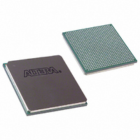
EP1S25F780C5 Altera, EP1S25F780C5 Datasheet - Page 92

EP1S25F780C5
Manufacturer Part Number
EP1S25F780C5
Description
IC STRATIX FPGA 25K LE 780-FBGA
Manufacturer
Altera
Series
Stratix®r
Datasheet
1.EP1S10F780C7.pdf
(276 pages)
Specifications of EP1S25F780C5
Number Of Logic Elements/cells
25660
Number Of Labs/clbs
2566
Total Ram Bits
1944576
Number Of I /o
597
Voltage - Supply
1.425 V ~ 1.575 V
Mounting Type
Surface Mount
Operating Temperature
0°C ~ 85°C
Package / Case
780-FBGA
Family Name
Stratix
Number Of Logic Blocks/elements
25660
# I/os (max)
597
Frequency (max)
500MHz
Process Technology
0.13um (CMOS)
Operating Supply Voltage (typ)
1.5V
Logic Cells
25660
Ram Bits
1944576
Operating Supply Voltage (min)
1.425V
Operating Supply Voltage (max)
1.575V
Operating Temp Range
0C to 85C
Operating Temperature Classification
Commercial
Mounting
Surface Mount
Pin Count
780
Package Type
FC-FBGA
Lead Free Status / RoHS Status
Contains lead / RoHS non-compliant
Number Of Gates
-
Lead Free Status / Rohs Status
Not Compliant
Other names
544-1120
Available stocks
Company
Part Number
Manufacturer
Quantity
Price
Company:
Part Number:
EP1S25F780C5
Manufacturer:
AT
Quantity:
186
Company:
Part Number:
EP1S25F780C5
Manufacturer:
ALTERA
Quantity:
315
Company:
Part Number:
EP1S25F780C5
Manufacturer:
ALTERA
Quantity:
3 000
Company:
Part Number:
EP1S25F780C5AA
Manufacturer:
ALTERA
Quantity:
269
Company:
Part Number:
EP1S25F780C5N
Manufacturer:
ALTERA
Quantity:
3 000
PLLs & Clock Networks
2–78
Stratix Device Handbook, Volume 1
Figure 2–45. EP1S30 Device Fast Regional Clock Pin Connections to Fast
Regional Clocks
Notes to
(1)
(2)
Combined Resources
Within each region, there are 22 distinct dedicated clocking resources
consisting of 16 global clock lines, four regional clock lines, and two fast
regional clock lines. Multiplexers are used with these clocks to form eight
bit busses to drive LAB row clocks, column IOE clocks, or row IOE clocks.
Another multiplexer is used at the LAB level to select two of the eight row
clocks to feed the LE registers within the LAB. See
This is a set of two multiplexers.
In addition to the FCLK pin inputs, there is also an input from the I/O interconnect.
(1), (2)
(1), (2)
Figure
FCLK3
FCLK1
2–45:
FCLK0
FCLK2
(1), (2)
(1), (2)
(1), (2)
(1), (2)
FCLK7
FCLK5
FCLK6
FCLK4
(1), (2)
(1), (2)
Figure
Altera Corporation
2–46.
fclk[1..0]
July 2005


