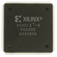
XC4013-6PQ240C Xilinx Inc, XC4013-6PQ240C Datasheet - Page 19

XC4013-6PQ240C
Manufacturer Part Number
XC4013-6PQ240C
Description
IC LOGIC CL ARRAY 13K GAT 240PQ
Manufacturer
Xilinx Inc
Series
XC4000r
Datasheet
1.XC4003-6PQ100C.pdf
(40 pages)
Specifications of XC4013-6PQ240C
Number Of Logic Elements/cells
1368
Number Of Labs/clbs
576
Total Ram Bits
18432
Number Of I /o
192
Number Of Gates
13000
Voltage - Supply
4.75 V ~ 5.25 V
Mounting Type
Surface Mount
Operating Temperature
0°C ~ 85°C
Package / Case
240-BFQFP
Lead Free Status / RoHS Status
Contains lead / RoHS non-compliant
Other names
122-1074
Available stocks
Company
Part Number
Manufacturer
Quantity
Price
Oscillator
An internal oscillator is used for clocking of the power-on
time-out, configuration memory clearing, and as the source
of CCLK in Master modes. This oscillator signal runs at a
nominal 8 MHz and varies with process, V
temperature between 10 MHz max and 4 MHz min. This
signal is available on an output control net (OSCO) in the
upper right corner of the chip, if the oscillator-run control bit
is enabled in the configuration memory. Two of four
resynchronized taps of the power-on time-out divider are
also available on OSC1 and OSC2. These taps are at the
fourth, ninth, fourteenth and nineteenth bits of the ripple
divider. This can provide output signals of approximately
500 kHz,16 kHz, 490 Hz and 15 Hz.
Special Purpose Pins
The mode pins are sampled prior to configuration to
determine the configuration mode and timing options. After
configuration, these pins can be used as auxiliary connec-
tions: Mode 0 (MD0.I) and Mode 2 (MD2.I) as inputs and
Mode 1 (MD1.O and MD1.T) as an output. The XACT
development system will not use these resources unless
they are explicitly specified in the design entry. These
dedicated nets are located in the lower left chip corner and
are near the readback nets. This allows convenient routing
if compatibility with the XC2000 and XC3000 family con-
ventions of M0/RT, M1/RD is desired.
Table 6. Configuration Modes
Master Serial
Slave Serial
Master Parallel up
Master Parallel down 1
Peripheral Synchr.
Peripheral Asynchr. 1
Reserved
Reserved
Peripheral Synchronous can be considered Slave Parallel
Mode
M2 M1 M0 CCLK
0
1
1
0
0
0
0
1
0
1
1
0
1
0
0 output
1 input
0 output
0 output
1 input
1 output
0 —
1 —
Data
Bit-Serial
Bit-Serial
Byte-Wide, 00000
Byte-Wide, 3FFFF
Byte-Wide
Byte-Wide
—
—
CC
and
2-25
Configuration
Configuration is the process of loading design-specific
programming data into one or more LCA devices to define
the functional operation of the internal blocks and their
interconnections. This is somewhat like loading the com-
mand registers of a programmable peripheral chip. The
XC4000 families use about 350 bits of configuration data
per CLB and its associated interconnects. Each configura-
tion bit defines the state of a static memory cell that
controls either a function look-up table bit, a multiplexer
input, or an interconnect pass transistor. The XACT devel-
opment system translates the design into a netlist file. It
automatically partitions, places and routes the logic and
generates the configuration data in PROM format.
Modes
The XC4000 families have six configuration modes se-
lected by a 3- bit input code applied to the M0, M1, and M2
inputs. There are three self-loading Master modes, two
Peripheral modes and the Serial Slave mode used prima-
rily for daisy-chained devices. During configuration, some
of the I/O pins are used temporarily for the configuration
process. See Table 6.
For a detailed description of these configuration modes,
see pages 2-32 through 2-41.
Master
The Master modes use an internal oscillator to generate
CCLK for driving potential slave devices, and to generate
address and timing for external PROM(s) containing the
configuration data. Master Parallel (up or down) modes
generate the CCLK signal and PROM addresses and
receive byte parallel data, which is internally serialized into
the LCA data-frame format. The up and down selection
generates starting addresses at either zero or 3FFFF, to
be compatible with different microprocessor addressing
conventions. The Master Serial mode generates CCLK
and receives the configuration data in serial form from a
Xilinx serial-configuration PROM.
Peripheral
The two Peripheral modes accept byte-wide data from a
bus. A READY/BUSY status is available as a handshake
signal. In the asynchronous mode, the internal oscillator
generates a CCLK burst signal that serializes the byte-
wide data. In the synchronous mode, an externally sup-
plied clock input to CCLK serializes the data.
Serial Slave
In the Serial Slave mode, the LCA device receives serial-
configuration data on the rising edge of CCLK and, after
loading its configuration, passes additional data out,
resynchronized on the next falling edge of CCLK. Multiple
slave devices with identical configurations can be wired
with parallel DIN inputs so that the devices can be config-
ured simultaneously.


