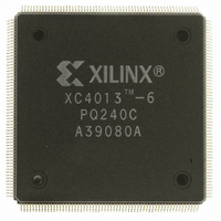
XC4013-6PQ240C Xilinx Inc, XC4013-6PQ240C Datasheet - Page 35

XC4013-6PQ240C
Manufacturer Part Number
XC4013-6PQ240C
Description
IC LOGIC CL ARRAY 13K GAT 240PQ
Manufacturer
Xilinx Inc
Series
XC4000r
Datasheet
1.XC4003-6PQ100C.pdf
(40 pages)
Specifications of XC4013-6PQ240C
Number Of Logic Elements/cells
1368
Number Of Labs/clbs
576
Total Ram Bits
18432
Number Of I /o
192
Number Of Gates
13000
Voltage - Supply
4.75 V ~ 5.25 V
Mounting Type
Surface Mount
Operating Temperature
0°C ~ 85°C
Package / Case
240-BFQFP
Lead Free Status / RoHS Status
Contains lead / RoHS non-compliant
Other names
122-1074
Available stocks
Company
Part Number
Manufacturer
Quantity
Price
Asynchronous Peripheral Mode Programming Switching Characteristics
A Low on the PROGRAM input is the more radical ap-
proach, and is recommended when the power-supply rise
time is excessive or poorly defined. As long as PROGRAM
is Low, the XC4000 device keeps clearing its configuration
memory. When PROGRAM goes High, the configuration
memory is cleared one more time, followed by the begin-
ning of configuration, provided the INIT input is not exter-
nally held Low. Note that a Low on the PROGRAM input
automatically forces a Low on the INIT output.
Notes:
RDY/BUSY
Write
RDY
RS, CS1
WS/CS0
D0-D7
CCLK
DOUT
1. Configuration must be delayed until the INIT of all LCA devices is High.
2. Time from end of WS to CCLK cycle for the new byte of data depends on completion of previous byte processing and
3. CCLK and DOUT timing is tested in slave mode.
4. T
Data need not be held beyond the rising edge of WS. BUSY will go active within 60 ns after the end of WS.
The shortest T
when a new word is loaded into the input register before the second-level buffer has started shifting out data.
the phase of the internal timing generator for CCLK.
BUSY
indicates that the double-buffered parallel-to-serial converter is not yet ready to receive new data.
(CS0, WS = Low, RS, CS1 = High)
DIN Setup time required
DIN Hold time required
RDY/BUSY delay after end of
Write or Read
RDY/BUSY active after begining of
Read
BUSY Low output (Note 4)
Effective Write time required
Earliest next WS after end of BUSY
Write to LCA
1 T
BUSY
Description
T
CA
WTRB
occurs when a byte is loaded into an empty parallel-to-serial converter. The longest T
2 T
WS may be asserted immediately after the end of BUSY.
This timing diagram shows very relaxed requirements:
DC
4
Previous Byte D6
3 T
CD
6 T
2-41
BUSY
1
2
3
4
7
5
6
Symbol
Using an open-collector or open-drain driver to hold INIT
Low before the beginning of configuration, causes the LCA
device to wait after having completed the configuration
memory clear operation. When INIT is no longer held Low
externally, the device determines its configuration mode
by capturing its status inputs, and is ready to start the
configuration process. A master device waits an additional
max 250 s to make sure that all slaves in the potential
daisy-chain have seen INIT being High.
T
T
T
T
T
T
CA
DC
CD
WTRB
RBWT
BUSY
D7
7
100
Min
D0
60
Read Status
0
0
2
READY
BUSY
D1
Max
4
60
60
9
D2
BUSY
RS, CS0
WS, CS1
D7
X6097
Units
CCLK
occurs
Periods
ns
ns
ns
ns
ns
ns


