EPF10K50EQC240-3N Altera, EPF10K50EQC240-3N Datasheet - Page 34
EPF10K50EQC240-3N
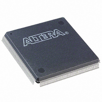
Manufacturer Part Number
EPF10K50EQC240-3N
Description
IC FLEX 10KE FPGA 50K 240-PQFP
Manufacturer
Altera
Series
FLEX-10KE®r
Datasheet
1.EPF10K30ETC144-3.pdf
(100 pages)
Specifications of EPF10K50EQC240-3N
Number Of Logic Elements/cells
2880
Number Of Labs/clbs
360
Total Ram Bits
40960
Number Of I /o
189
Number Of Gates
199000
Voltage - Supply
2.3 V ~ 2.7 V
Mounting Type
Surface Mount
Operating Temperature
0°C ~ 85°C
Package / Case
240-MQFP, 240-PQFP
Family Name
FLEX 10KE
Number Of Usable Gates
50000
Number Of Logic Blocks/elements
2880
# Registers
189
# I/os (max)
189
Frequency (max)
166.67MHz
Process Technology
CMOS
Operating Supply Voltage (typ)
2.5V
Logic Cells
2880
Ram Bits
40960
Device System Gates
199000
Operating Supply Voltage (min)
2.3V
Operating Supply Voltage (max)
2.7V
Operating Temp Range
0C to 85C
Operating Temperature Classification
Commercial
Mounting
Surface Mount
Pin Count
240
Package Type
PQFP
Lead Free Status / RoHS Status
Lead free / RoHS Compliant
Available stocks
Company
Part Number
Manufacturer
Quantity
Price

Part Number:
EPF10K50EQC240-3N
Manufacturer:
ALTERA
Quantity:
20 000


FLEX 10KE Embedded Programmable Logic Devices Data Sheet
34
Table 9. Peripheral Bus Sources for EPF10K100E, EPF10K130E, EPF10K200E & EPF10K200S Devices
OE0
OE1
OE2
OE3
OE4
OE5
CLKENA0/CLK0/GLOBAL0
CLKENA1/OE6/GLOBAL1
CLKENA2/CLR0
CLKENA3/OE7/GLOBAL2
CLKENA4/CLR1
CLKENA5/CLK1/GLOBAL3
Control Signal
Peripheral
Signals on the peripheral control bus can also drive the four global signals,
referred to as GLOBAL0 through GLOBAL3 in
generated signal can drive a global signal, providing the same low-skew,
low-delay characteristics as a signal driven by an input pin. An LE drives
the global signal by driving a row line that drives the peripheral bus,
which then drives the global signal. This feature is ideal for internally
generated clear or clock signals with high fan-out. However, internally
driven global signals offer no advantage over the general-purpose
interconnect for routing data signals. The dedicated input pin should be
driven to a known logic state (such as ground) and not be allowed to float.
The chip-wide output enable pin is an active-high pin (DEV_OE) that can
be used to tri-state all pins on the device. This option can be set in the
Altera software. On EPF10K50E and EPF10K200E devices, the built-in I/O
pin pull-up resistors (which are active during configuration) are active
when the chip-wide output enable pin is asserted. The registers in the IOE
can also be reset by the chip-wide reset pin.
EPF10K100E
Row A
Row C
Row E
Row L
Row I
Row K
Row F
Row D
Row B
Row H
Row J
Row G
EPF10K130E
Row C
Row E
Row G
Row N
Row K
Row M
Row H
Row F
Row D
Row J
Row L
Row I
Tables 8
and 9. An internally
Altera Corporation
EPF10K200S
EPF10K200E
Row G
Row I
Row K
Row R
Row O
Row Q
Row L
Row J
Row H
Row N
Row P
Row M
Related parts for EPF10K50EQC240-3N
Image
Part Number
Description
Manufacturer
Datasheet
Request
R

Part Number:
Description:
CYCLONE II STARTER KIT EP2C20N
Manufacturer:
Altera
Datasheet:


Part Number:
Description:
CPLD, EP610 Family, ECMOS Process, 300 Gates, 16 Macro Cells, 16 Reg., 16 User I/Os, 5V Supply, 35 Speed Grade, 24DIP
Manufacturer:
Altera Corporation
Datasheet:
Part Number:
Description:
CPLD, EP610 Family, ECMOS Process, 300 Gates, 16 Macro Cells, 16 Reg., 16 User I/Os, 5V Supply, 15 Speed Grade, 24DIP
Manufacturer:
Altera Corporation
Datasheet:
Part Number:
Description:
Manufacturer:
Altera Corporation
Datasheet:
Part Number:
Description:
CPLD, EP610 Family, ECMOS Process, 300 Gates, 16 Macro Cells, 16 Reg., 16 User I/Os, 5V Supply, 30 Speed Grade, 24DIP
Manufacturer:
Altera Corporation
Datasheet:
Part Number:
Description:
High-performance, low-power erasable programmable logic devices with 8 macrocells, 10ns
Manufacturer:
Altera Corporation
Datasheet:
Part Number:
Description:
High-performance, low-power erasable programmable logic devices with 8 macrocells, 7ns
Manufacturer:
Altera Corporation
Datasheet:
Part Number:
Description:
Classic EPLD
Manufacturer:
Altera Corporation
Datasheet:
Part Number:
Description:
High-performance, low-power erasable programmable logic devices with 8 macrocells, 10ns
Manufacturer:
Altera Corporation
Datasheet:
Part Number:
Description:
Manufacturer:
Altera Corporation
Datasheet:
Part Number:
Description:
Manufacturer:
Altera Corporation
Datasheet:
Part Number:
Description:
Manufacturer:
Altera Corporation
Datasheet:
Part Number:
Description:
CPLD, EP610 Family, ECMOS Process, 300 Gates, 16 Macro Cells, 16 Reg., 16 User I/Os, 5V Supply, 25 Speed Grade, 24DIP
Manufacturer:
Altera Corporation
Datasheet: