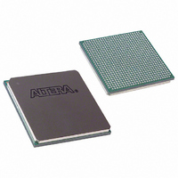
EP4CE115F29I8LN Altera, EP4CE115F29I8LN Datasheet - Page 85

EP4CE115F29I8LN
Manufacturer Part Number
EP4CE115F29I8LN
Description
IC CYCLONE IV FPGA 115K 780-FBGA
Manufacturer
Altera
Series
CYCLONE® IV Er
Datasheets
1.EP4CGX15BN11C8N.pdf
(44 pages)
2.EP4CGX15BN11C8N.pdf
(14 pages)
3.EP4CGX15BN11C8N.pdf
(478 pages)
4.EP4CGX15BN11C8N.pdf
(10 pages)
Specifications of EP4CE115F29I8LN
Number Of Logic Elements/cells
114480
Number Of Labs/clbs
7155
Total Ram Bits
3888000
Number Of I /o
528
Voltage - Supply
0.97 V ~ 1.03 V
Mounting Type
Surface Mount
Operating Temperature
-40°C ~ 100°C
Package / Case
780-FBGA
Lead Free Status / RoHS Status
Lead free / RoHS Compliant
Number Of Gates
-
Available stocks
Company
Part Number
Manufacturer
Quantity
Price
- EP4CGX15BN11C8N PDF datasheet
- EP4CGX15BN11C8N PDF datasheet #2
- EP4CGX15BN11C8N PDF datasheet #3
- EP4CGX15BN11C8N PDF datasheet #4
- Current page: 85 of 478
- Download datasheet (13Mb)
Chapter 5: Clock Networks and PLLs in Cyclone IV Devices
Clock Feedback Modes
No Compensation Mode
© December 2010 Altera Corporation
In no compensation mode, the PLL does not compensate for any clock networks. This
provides better jitter performance because clock feedback into the PFD does not pass
through as much circuitry. Both the PLL internal and external clock outputs are phase
shifted with respect to the PLL clock input.
Figure 5–13
this mode.
Figure 5–13. Phase Relationship Between PLL Clocks in No Compensation Mode
Notes to
(1) Internal clocks fed by the PLL are phase
(2) The PLL clock outputs can lead or lag the PLL input clocks.
Figure
shows a waveform example of the phase relationship of the PLL clock in
5–13:
PLL Reference
Clock at the Input Pin
PLL Clock at the
Register Clock Port
(1), (2)
External PLL Clock
Outputs
(2)
Phase Aligned
-
aligned to each other.
Cyclone IV Device Handbook, Volume 1
5–23
Related parts for EP4CE115F29I8LN
Image
Part Number
Description
Manufacturer
Datasheet
Request
R

Part Number:
Description:
CYCLONE II STARTER KIT EP2C20N
Manufacturer:
Altera
Datasheet:

Part Number:
Description:
CPLD, EP610 Family, ECMOS Process, 300 Gates, 16 Macro Cells, 16 Reg., 16 User I/Os, 5V Supply, 35 Speed Grade, 24DIP
Manufacturer:
Altera Corporation
Datasheet:

Part Number:
Description:
CPLD, EP610 Family, ECMOS Process, 300 Gates, 16 Macro Cells, 16 Reg., 16 User I/Os, 5V Supply, 15 Speed Grade, 24DIP
Manufacturer:
Altera Corporation
Datasheet:

Part Number:
Description:
Manufacturer:
Altera Corporation
Datasheet:

Part Number:
Description:
CPLD, EP610 Family, ECMOS Process, 300 Gates, 16 Macro Cells, 16 Reg., 16 User I/Os, 5V Supply, 30 Speed Grade, 24DIP
Manufacturer:
Altera Corporation
Datasheet:

Part Number:
Description:
High-performance, low-power erasable programmable logic devices with 8 macrocells, 10ns
Manufacturer:
Altera Corporation
Datasheet:

Part Number:
Description:
High-performance, low-power erasable programmable logic devices with 8 macrocells, 7ns
Manufacturer:
Altera Corporation
Datasheet:

Part Number:
Description:
Classic EPLD
Manufacturer:
Altera Corporation
Datasheet:

Part Number:
Description:
High-performance, low-power erasable programmable logic devices with 8 macrocells, 10ns
Manufacturer:
Altera Corporation
Datasheet:

Part Number:
Description:
Manufacturer:
Altera Corporation
Datasheet:

Part Number:
Description:
Manufacturer:
Altera Corporation
Datasheet:

Part Number:
Description:
Manufacturer:
Altera Corporation
Datasheet:

Part Number:
Description:
CPLD, EP610 Family, ECMOS Process, 300 Gates, 16 Macro Cells, 16 Reg., 16 User I/Os, 5V Supply, 25 Speed Grade, 24DIP
Manufacturer:
Altera Corporation
Datasheet:


