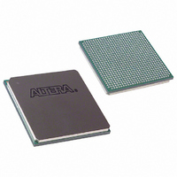
EP3C120F780I7 Altera, EP3C120F780I7 Datasheet - Page 121

EP3C120F780I7
Manufacturer Part Number
EP3C120F780I7
Description
IC CYCLONE III FPGA 120K 780FBGA
Manufacturer
Altera
Series
Cyclone® IIIr
Datasheets
1.EP3C5F256C8N.pdf
(5 pages)
2.EP3C5F256C8N.pdf
(34 pages)
3.EP3C5F256C8N.pdf
(66 pages)
4.EP3C5F256C8N.pdf
(14 pages)
5.EP3C5F256C8N.pdf
(76 pages)
6.EP3C120F780I7.pdf
(274 pages)
Specifications of EP3C120F780I7
Number Of Logic Elements/cells
119088
Number Of Labs/clbs
7443
Total Ram Bits
3981312
Number Of I /o
531
Voltage - Supply
1.15 V ~ 1.25 V
Mounting Type
Surface Mount
Operating Temperature
-40°C ~ 100°C
Package / Case
780-FBGA
Family Name
Cyclone III
Number Of Logic Blocks/elements
119088
# I/os (max)
531
Frequency (max)
437.5MHz
Process Technology
65nm
Operating Supply Voltage (typ)
1.2V
Logic Cells
119088
Ram Bits
3981312
Operating Supply Voltage (min)
1.15V
Operating Supply Voltage (max)
1.25V
Operating Temp Range
-40C to 100C
Operating Temperature Classification
Industrial
Mounting
Surface Mount
Pin Count
780
Package Type
FBGA
For Use With
544-2589 - KIT DEV EMB CYCLONE III EDITION544-2566 - KIT DEV DSP CYCLONE III EDITION544-2444 - KIT DEV CYCLONE III EP3C120
Lead Free Status / RoHS Status
Contains lead / RoHS non-compliant
Number Of Gates
-
Lead Free Status / Rohs Status
Not Compliant
Available stocks
Company
Part Number
Manufacturer
Quantity
Price
Part Number:
EP3C120F780I7
Manufacturer:
ALTERA/阿尔特拉
Quantity:
20 000
Company:
Part Number:
EP3C120F780I7N
Manufacturer:
ALTERA
Quantity:
118
Chapter 6: I/O Features in the Cyclone III Device Family
Pad Placement and DC Guidelines
Pad Placement and DC Guidelines
Pad Placement
DC Guidelines
Chapter Revision History
Table 6–7. Chapter Revision History (Part 1 of 3)
© December 2009
December 2009
July 2009
June 2009
October 2008
Date
f
Altera Corporation
Altera recommends that you create a Quartus II design, enter your device I/O
assignments, and compile your design to validate your pin placement. The Quartus II
software checks your pin connections with respect to the I/O assignment and
placement rules to ensure proper device operation. These rules are dependent on
device density, package, I/O assignments, voltage assignments, and other factors that
are not fully described in this chapter.
For more information about how the Quartus II software checks I/O restrictions, refer
to the
For the Quartus II software to automatically check for illegally placed pads according
to the DC guidelines, set the DC current sink or source value to Electromigration
Current assignment on each of the output pins that are connected to the external
resistive load.
The programmable current strength setting has an impact on the amount of DC
current that an output pin can source or sink. Determine if the current strength setting
is sufficient for the external resistive load condition on the output pin.
Table 6–7
Version
3.2
3.1
3.0
2.1
I/O Management
lists the revision history for this chapter.
Minor changes to the text.
Made minor correction to the part number.
Updated to include Cyclone III LS information
■
■
■
■
■
■
■
■
■
Updated chapter part number.
Updated “Introduction” on page 6–1, “PCI-Clamp Diode” on page 6–6, “On-
Chip Series Termination Without Calibration” on page 6–10, “I/O Standards”
on page 6–11, “I/O Banks” on page 6–16, “High-Speed Differential
Interfaces” on page 6–20, and “External Memory Interfacing” on page 6–20.
Updated Table 6–6 on page 6–18.
Added (Note 6) to Table 6–5.
Updated the “I/O Banks” section.
Updated the “Differential Pad Placement Guidelines” section.
Updated the “V
Removed any mention of “RSDS and PPDS are registered trademarks of
National Semiconductor” from chapter.
Updated chapter to new template.
chapter in volume 2 of the Quartus II Handbook.
REF
Pad Placement Guidelines” section.
Changes Made
Cyclone III Device Handbook, Volume 1
6–21


