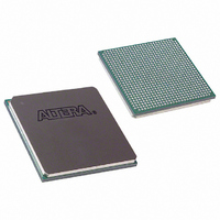
EP1S25F780C6 Altera, EP1S25F780C6 Datasheet - Page 127

EP1S25F780C6
Manufacturer Part Number
EP1S25F780C6
Description
IC STRATIX FPGA 25K LE 780-FBGA
Manufacturer
Altera
Series
Stratix®r
Datasheet
1.EP1S10F780C7.pdf
(276 pages)
Specifications of EP1S25F780C6
Number Of Logic Elements/cells
25660
Number Of Labs/clbs
2566
Total Ram Bits
1944576
Number Of I /o
597
Voltage - Supply
1.425 V ~ 1.575 V
Mounting Type
Surface Mount
Operating Temperature
0°C ~ 85°C
Package / Case
780-FBGA
Family Name
Stratix
Number Of Logic Blocks/elements
25660
# I/os (max)
597
Frequency (max)
450.05MHz
Process Technology
0.13um (CMOS)
Operating Supply Voltage (typ)
1.5V
Logic Cells
25660
Ram Bits
1944576
Operating Supply Voltage (min)
1.425V
Operating Supply Voltage (max)
1.575V
Operating Temp Range
0C to 85C
Operating Temperature Classification
Commercial
Mounting
Surface Mount
Pin Count
780
Package Type
FC-FBGA
Lead Free Status / RoHS Status
Contains lead / RoHS non-compliant
Number Of Gates
-
Lead Free Status / Rohs Status
Not Compliant
Other names
544-1121
Available stocks
Company
Part Number
Manufacturer
Quantity
Price
Company:
Part Number:
EP1S25F780C6
Manufacturer:
ALTERA
Quantity:
10
Company:
Part Number:
EP1S25F780C6
Manufacturer:
ALTERA
Quantity:
246
Part Number:
EP1S25F780C6
Manufacturer:
ALTERA/阿尔特拉
Quantity:
20 000
Part Number:
EP1S25F780C6ES
Manufacturer:
ALTERA
Quantity:
20 000
Company:
Part Number:
EP1S25F780C6N
Manufacturer:
ALTERA
Quantity:
1 045
Figure 2–66. Input Timing Diagram in DDR Mode
Altera Corporation
July 2005
Input To
Logic Array
Data at
input pin
CLK
A'
B'
When using the IOE for DDR outputs, the two output registers are
configured to clock two data paths from LEs on rising clock edges. These
output registers are multiplexed by the clock to drive the output pin at a
×2 rate. One output register clocks the first bit out on the clock high time,
while the other output register clocks the second bit out on the clock low
time.
shows the DDR output timing diagram.
A0
Figure 2–67
B1
A1
B2
shows the IOE configured for DDR output.
A1
B1
A2
B3
A2
B2
A3
B4
A3
B3
Stratix Device Handbook, Volume 1
Stratix Architecture
Figure 2–68
2–113


