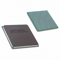
EP1SGX25CF672C6 Altera, EP1SGX25CF672C6 Datasheet - Page 239

EP1SGX25CF672C6
Manufacturer Part Number
EP1SGX25CF672C6
Description
IC STRATIX GX FPGA 25KLE 672FBGA
Manufacturer
Altera
Series
Stratix® GXr
Datasheet
1.EP1SGX10CF672C7N.pdf
(272 pages)
Specifications of EP1SGX25CF672C6
Number Of Logic Elements/cells
25660
Number Of Labs/clbs
2566
Total Ram Bits
1944576
Number Of I /o
455
Voltage - Supply
1.425 V ~ 1.575 V
Mounting Type
Surface Mount
Operating Temperature
0°C ~ 85°C
Package / Case
672-FBGA
Family Name
Stratix GX
Number Of Logic Blocks/elements
25660
# I/os (max)
455
Frequency (max)
5GHz
Process Technology
SRAM
Operating Supply Voltage (typ)
1.5V
Logic Cells
25660
Ram Bits
1944576
Operating Supply Voltage (min)
1.425V
Operating Supply Voltage (max)
1.575V
Operating Temp Range
0C to 85C
Operating Temperature Classification
Commercial
Mounting
Surface Mount
Pin Count
672
Package Type
FC-FBGA
Lead Free Status / RoHS Status
Contains lead / RoHS non-compliant
Number Of Gates
-
Lead Free Status / Rohs Status
Not Compliant
Available stocks
Company
Part Number
Manufacturer
Quantity
Price
Company:
Part Number:
EP1SGX25CF672C6
Manufacturer:
ALTERA
Quantity:
3 000
Part Number:
EP1SGX25CF672C6
Manufacturer:
ALTERA/阿尔特拉
Quantity:
20 000
Company:
Part Number:
EP1SGX25CF672C6ES
Manufacturer:
ALTERA
Quantity:
5
Altera Corporation
June 2006
Notes to
(1)
(2)
t
t
t
t
t
t
t
t
t
t
INSU
INH
OUTCO
INSUPLL
INHPLL
OUTCOPLL
INSU
INH
OUTCO
INSUPLL
Table 6–52. Stratix GX Regional Clock External I/O Timing Parameters
Table 6–53. Stratix GX Global Clock External I/O Timing Parameters (Part 1 of 2)
Symbol
Symbol
These timing parameters are sample-tested only.
These timing parameters are for column IOE pins. Row IOE pins are 100- to 250-ps slower depending on device,
speed grade, and the specific parameter in question. You should use the Quartus II software to verify the external
timing for any pin.
Table
6–52:
Setup time for input or bidirectional pin using column IOE
input register with regional clock fed by
Hold time for input or bidirectional pin using column IOE
input register with regional clock fed by
Clock-to-output delay output or bidirectional pin using
column IOE output register with regional clock fed by
pin
Setup time for input or bidirectional pin using column IOE
input register with regional clock fed by Enhanced PLL with
default phase setting
Hold time for input or bidirectional pin using column IOE
input register with regional clock fed by Enhanced PLL with
default phase setting
Clock-to-output delay output or bidirectional pin using
column IOE output register with regional clock Enhanced
PLL with default phase setting
Setup time for input or bidirectional pin using column IOE
input register with global clock fed by
Hold time for input or bidirectional pin using column IOE
input register with global clock fed by
Clock-to-output delay output or bidirectional pin using
column IOE output register with global clock fed by
Setup time for input or bidirectional pin using column IOE
input register with global clock fed by Enhanced PLL with
default phase setting
Table 6–52
regional clock networks.
Table 6–53
clock networks.
Parameter
Parameter
shows the external I/O timing parameters when using global
shows the external I/O timing parameters when using
CLK
CLK
CLK
CLK
pin
pin
pin
pin
CLK
Stratix GX Device Handbook, Volume 1
CLK
pin
DC & Switching Characteristics
C
C
C
Notes
L O A D
L O A D
L O A D
(1),
= 10 pF
= 10 pF
= 10 pF
Conditions
Conditions
(2)
Notes
(1),
(2)
6–37


