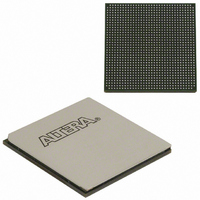
EP2SGX90EF1152C3N Altera, EP2SGX90EF1152C3N Datasheet - Page 76

EP2SGX90EF1152C3N
Manufacturer Part Number
EP2SGX90EF1152C3N
Description
IC STRATIX II GX 90K 1152-FBGA
Manufacturer
Altera
Series
Stratix® II GXr
Datasheet
1.EP2SGX90EF1152C3N.pdf
(316 pages)
Specifications of EP2SGX90EF1152C3N
Number Of Logic Elements/cells
90960
Number Of Labs/clbs
4548
Total Ram Bits
4520448
Number Of I /o
558
Voltage - Supply
1.15 V ~ 1.25 V
Mounting Type
Surface Mount
Operating Temperature
0°C ~ 70°C
Package / Case
1152-FBGA
Family Name
Stratix II GX
Number Of Logic Blocks/elements
90960
# I/os (max)
558
Frequency (max)
816.9MHz
Process Technology
SRAM
Operating Supply Voltage (typ)
1.2V
Logic Cells
90960
Ram Bits
4520448
Operating Supply Voltage (min)
1.15V
Operating Supply Voltage (max)
1.25V
Operating Temp Range
0C to 85C
Operating Temperature Classification
Commercial
Mounting
Surface Mount
Pin Count
1152
Package Type
FC-FBGA
For Use With
544-1725 - PCIE KIT W/S II GX EP2SGX90N544-1724 - SI KIT W/SII GX EP2SGX90N544-1702 - VIDEO KIT W/SII GX EP2SGX90N
Lead Free Status / RoHS Status
Lead free / RoHS Compliant
Number Of Gates
-
Lead Free Status / Rohs Status
Compliant
Other names
544-1766
EP2SGX90EF35C3NES
EP2SGX90EF35C3NES
Available stocks
Company
Part Number
Manufacturer
Quantity
Price
Part Number:
EP2SGX90EF1152C3N
Manufacturer:
ALTERA/阿尔特拉
Quantity:
20 000
- Current page: 76 of 316
- Download datasheet (2Mb)
MultiTrack Interconnect
2–68
Stratix II GX Device Handbook, Volume 1
Shared arithmetic chain
Carry chain
Register chain
Local interconnect
Direct link interconnect
R4 interconnect
R24 interconnect
C4 interconnect
C16 interconnect
ALM
M512 RAM block
M4K RAM block
M-RAM block
DSP blocks
Table 2–18. Stratix II GX Device Routing Scheme (Part 1 of 2)
Source
C16 column interconnects span a length of 16 LABs and provide the
fastest resource for long column connections between LABs, TriMatrix
memory blocks, DSP blocks, and IOEs. C16 interconnects can cross
M-RAM blocks and also drive to row and column interconnects at every
fourth LAB. C16 interconnects drive LAB local interconnects via C4 and
R4 interconnects and do not drive LAB local interconnects directly. All
embedded blocks communicate with the logic array similar to
LAB-to-LAB interfaces. Each block (that is, TriMatrix memory and DSP
blocks) connects to row and column interconnects and has local
interconnect regions driven by row and column interconnects. These
blocks also have direct link interconnects for fast connections to and from
a neighboring LAB. All blocks are fed by the row LAB clocks,
labclk[5..0].
Table 2–18
v v v v v v
shows the Stratix II GX device’s routing scheme.
v
v
v
v v v
v v v
v v v v
v v
v v v v
v v v v
v
v v v v
Destination
v
v
v
v
v
v
v
v
v v v v v v v
Altera Corporation
October 2007
Related parts for EP2SGX90EF1152C3N
Image
Part Number
Description
Manufacturer
Datasheet
Request
R

Part Number:
Description:
CYCLONE II STARTER KIT EP2C20N
Manufacturer:
Altera
Datasheet:

Part Number:
Description:
CPLD, EP610 Family, ECMOS Process, 300 Gates, 16 Macro Cells, 16 Reg., 16 User I/Os, 5V Supply, 35 Speed Grade, 24DIP
Manufacturer:
Altera Corporation
Datasheet:

Part Number:
Description:
CPLD, EP610 Family, ECMOS Process, 300 Gates, 16 Macro Cells, 16 Reg., 16 User I/Os, 5V Supply, 15 Speed Grade, 24DIP
Manufacturer:
Altera Corporation
Datasheet:

Part Number:
Description:
Manufacturer:
Altera Corporation
Datasheet:

Part Number:
Description:
CPLD, EP610 Family, ECMOS Process, 300 Gates, 16 Macro Cells, 16 Reg., 16 User I/Os, 5V Supply, 30 Speed Grade, 24DIP
Manufacturer:
Altera Corporation
Datasheet:

Part Number:
Description:
High-performance, low-power erasable programmable logic devices with 8 macrocells, 10ns
Manufacturer:
Altera Corporation
Datasheet:

Part Number:
Description:
High-performance, low-power erasable programmable logic devices with 8 macrocells, 7ns
Manufacturer:
Altera Corporation
Datasheet:

Part Number:
Description:
Classic EPLD
Manufacturer:
Altera Corporation
Datasheet:

Part Number:
Description:
High-performance, low-power erasable programmable logic devices with 8 macrocells, 10ns
Manufacturer:
Altera Corporation
Datasheet:

Part Number:
Description:
Manufacturer:
Altera Corporation
Datasheet:

Part Number:
Description:
Manufacturer:
Altera Corporation
Datasheet:

Part Number:
Description:
Manufacturer:
Altera Corporation
Datasheet:

Part Number:
Description:
CPLD, EP610 Family, ECMOS Process, 300 Gates, 16 Macro Cells, 16 Reg., 16 User I/Os, 5V Supply, 25 Speed Grade, 24DIP
Manufacturer:
Altera Corporation
Datasheet:


