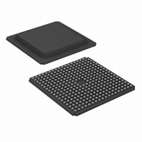
XC3S1200E-4FGG320I Xilinx Inc, XC3S1200E-4FGG320I Datasheet - Page 130

XC3S1200E-4FGG320I
Manufacturer Part Number
XC3S1200E-4FGG320I
Description
IC FPGA SPARTAN-3E 1200K 320FBGA
Manufacturer
Xilinx Inc
Series
Spartan™-3Er
Datasheet
1.XC3S100E-4VQG100C.pdf
(233 pages)
Specifications of XC3S1200E-4FGG320I
Number Of Logic Elements/cells
19512
Number Of Labs/clbs
2168
Total Ram Bits
516096
Number Of I /o
250
Number Of Gates
1200000
Voltage - Supply
1.14 V ~ 1.26 V
Mounting Type
Surface Mount
Operating Temperature
-40°C ~ 100°C
Package / Case
320-BGA
Lead Free Status / RoHS Status
Lead free / RoHS Compliant
Available stocks
Company
Part Number
Manufacturer
Quantity
Price
Company:
Part Number:
XC3S1200E-4FGG320I
Manufacturer:
Xilinx Inc
Quantity:
10 000
Part Number:
XC3S1200E-4FGG320I
Manufacturer:
XILINX/赛灵思
Quantity:
20 000
- Current page: 130 of 233
- Download datasheet (6Mb)
DC and Switching Characteristics
Table 90: Propagation Times for the IOB Input Path
Table 91: Input Timing Adjustments by IOSTANDARD
130
Notes:
1.
2.
Single-Ended Standards
LVTTL
LVCMOS33
LVCMOS25
LVCMOS18
LVCMOS15
LVCMOS12
PCI33_3
PCI66_3
HSTL_I_18
HSTL_III_18
SSTL18_I
SSTL2_I
Propagation Times
Following Signal Standard
Convert Input Time from
Symbol
T
T
IOPLID
The numbers in this table are tested using the methodology presented in
Table 77
This propagation time requires adjustment whenever a signal standard other than LVCMOS25 is assigned to the data Input. When this is
true, add the appropriate Input adjustment from
IOPLI
LVCMOS25 to the
(IOSTANDARD)
and
The time it takes for data to
travel from the Input pin
through the IFF latch to the
I output with no input delay
programmed
The time it takes for data to
travel from the Input pin
through the IFF latch to the
I output with the input delay
programmed
Table
80.
Description
Adjustment Below
0.42
0.42
0.96
0.62
0.26
0.41
0.41
0.12
0.17
0.30
0.15
-5
Speed Grade
0
Add the
0.12
0.43
0.43
0.98
0.63
0.27
0.42
0.42
0.17
0.30
0.15
LVCMOS25
IFD_DELAY_VALUE = 0
LVCMOS25
IFD_DELAY_VALUE =
default software setting
-4
0
Table
Conditions
91.
Units
ns
ns
ns
ns
ns
ns
ns
ns
ns
ns
ns
ns
www.xilinx.com
(2)
(2)
,
,
Table 91: Input Timing Adjustments by IOSTANDARD
Notes:
1.
2.
Differential Standards
LVDS_25
BLVDS_25
MINI_LVDS_25
LVPECL_25
RSDS_25
DIFF_HSTL_I_18
DIFF_HSTL_III_18
DIFF_SSTL18_I
DIFF_SSTL2_I
Following Signal Standard
Convert Input Time from
Table 95
The numbers in this table are tested using the methodology
presented in
set forth in
These adjustments are used to convert input path times originally
specified for the LVCMOS25 standard to times that correspond to
other signal standards.
LVCMOS25 to the
DELAY_
VALUE=
(IOSTANDARD)
IFD_
0
2
3
and are based on the operating conditions set forth in
Table
XC3S100E
Table 95
All Others
Device
77,
All
Table
and are based on the operating conditions
80, and
Adjustment Below
DS312-3 (v3.8) August 26, 2009
Max
1.96
5.40
6.30
0.48
0.39
0.48
0.27
0.48
0.48
0.48
0.30
0.32
Speed Grade
-5
-5
Speed Grade
Table
Add the
Product Specification
82.
Max
2.25
5.97
7.20
0.49
0.39
0.49
0.27
0.49
0.49
0.49
0.30
0.32
-4
-4
Units
Units
ns
ns
ns
ns
ns
ns
ns
ns
ns
ns
ns
R
Related parts for XC3S1200E-4FGG320I
Image
Part Number
Description
Manufacturer
Datasheet
Request
R

Part Number:
Description:
IC SPARTAN-3E FPGA 1200K 400FBGA
Manufacturer:
Xilinx Inc
Datasheet:

Part Number:
Description:
FPGA Spartan®-3E Family 1.2M Gates 19512 Cells 572MHz 90nm (CMOS) Technology 1.2V 256-Pin FTBGA
Manufacturer:
Xilinx Inc
Datasheet:

Part Number:
Description:
IC SPARTAN-3E FPGA 1200K 320FBGA
Manufacturer:
Xilinx Inc
Datasheet:

Part Number:
Description:
IC FPGA SPARTAN3E 1200K 256FTBGA
Manufacturer:
Xilinx Inc
Datasheet:

Part Number:
Description:
IC FPGA SPARTAN3E 1200K 256FTBGA
Manufacturer:
Xilinx Inc
Datasheet:

Part Number:
Description:
IC FPGA SPARTAN-3E 1200K 320FBGA
Manufacturer:
Xilinx Inc
Datasheet:

Part Number:
Description:
IC FPGA SPARTAN-3E 1200K 400FBGA
Manufacturer:
Xilinx Inc
Datasheet:

Part Number:
Description:
IC FPGA SPARTAN-3E 1200K 400FBGA
Manufacturer:
Xilinx Inc
Datasheet:

Part Number:
Description:
IC FPGA SPARTAN 3E 256FTBGA
Manufacturer:
Xilinx Inc
Datasheet:

Part Number:
Description:
IC FPGA SPARTAN 3E 320FBGA
Manufacturer:
Xilinx Inc
Datasheet:

Part Number:
Description:
PROGRAMMABLE INTEGRATED CIRCUIT
Manufacturer:
Xilinx Inc

Part Number:
Description:
FPGA Spartan®-3E Family 1.2M Gates 19512 Cells 572MHz 90nm (CMOS) Technology 1.2V 400-Pin FBGA
Manufacturer:
Xilinx Inc
Datasheet:

Part Number:
Description:
FPGA Spartan®-3E Family 1.2M Gates 19512 Cells 572MHz 90nm (CMOS) Technology 1.2V 256-Pin FTBGA
Manufacturer:
Xilinx Inc
Datasheet:

Part Number:
Description:
FPGA Spartan®-3E Family 1.2M Gates 19512 Cells 572MHz 90nm (CMOS) Technology 1.2V 320-Pin FBGA
Manufacturer:
Xilinx Inc
Datasheet:

Part Number:
Description:
IC CPLD .8K 36MCELL 44-VQFP
Manufacturer:
Xilinx Inc
Datasheet:


