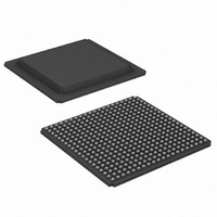
XA3S700A-4FGG400I Xilinx Inc, XA3S700A-4FGG400I Datasheet - Page 41

XA3S700A-4FGG400I
Manufacturer Part Number
XA3S700A-4FGG400I
Description
IC FPGA SPARTAN-3A 700K 400-FBGA
Manufacturer
Xilinx Inc
Series
Spartan™-3A XAr
Datasheet
1.XA3S200A-4FTG256I.pdf
(56 pages)
Specifications of XA3S700A-4FGG400I
Number Of Logic Elements/cells
13248
Number Of Labs/clbs
1472
Total Ram Bits
368640
Number Of I /o
311
Number Of Gates
700000
Voltage - Supply
1.14 V ~ 1.26 V
Mounting Type
Surface Mount
Operating Temperature
-40°C ~ 100°C
Package / Case
400-BGA
Lead Free Status / RoHS Status
Lead free / RoHS Compliant
Available stocks
Company
Part Number
Manufacturer
Quantity
Price
Company:
Part Number:
XA3S700A-4FGG400I
Manufacturer:
XILINX
Quantity:
624
Company:
Part Number:
XA3S700A-4FGG400I
Manufacturer:
Xilinx Inc
Quantity:
10 000
Part Number:
XA3S700A-4FGG400I
Manufacturer:
XILINX/赛灵思
Quantity:
20 000
Digital Frequency Synthesizer
Table 37: Recommended Operating Conditions for the DFS
Table 38: Switching Characteristics for the DFS
DS681 (v1.1) February 3, 2009
Product Specification
Notes:
1.
2.
3.
Output Frequency Ranges
CLKOUT_FREQ_FX
Output Clock Jitter
CLKOUT_PER_JITT_FX
Duty Cycle
CLKOUT_DUTY_CYCLE_FX Duty cycle precision for the CLKFX and CLKFX180 outputs,
Phase Alignment
CLKOUT_PHASE_FX
CLKOUT_PHASE_FX180
Input Frequency Ranges
F
Input Clock Jitter Tolerance
CLKIN_CYC_JITT_FX_LF
CLKIN_CYC_JITT_FX_HF
CLKIN_PER_JITT_FX
CLKIN
DFS specifications apply when either of the DFS outputs (CLKFX or CLKFX180) are used.
If both DFS and DLL outputs are used on the same DCM, follow the more restrictive CLKIN_FREQ_DLL specifications
in
CLKIN input jitter beyond these limits may cause the DCM to lose lock.
Table
Symbol
(5,6)
CLKIN_FREQ_FX
35.
Symbol
R
(6)
(3,4)
(2)
(2)
(3)
Frequency for the CLKFX and CLKFX180 outputs
Period jitter at the CLKFX and CLKFX180
outputs.
including the BUFGMUX and clock tree duty-cycle distortion
Phase offset between the DFS CLKFX output and the DLL CLK0
output when both the DFS and DLL are used
Phase offset between the DFS CLKFX180 output and the DLL
CLK0 output when both the DFS and DLL are used
Frequency for the CLKIN input
Cycle-to-cycle jitter at the CLKIN
input, based on CLKFX output
frequency
Period jitter at the CLKIN input
Description
Description
www.xilinx.com
F
F
CLKFX
CLKFX
> 20 MHz
≤
CLKIN
CLKIN
20 MHz
< 150 MHz
> 150 MHz
Device
All
All
All
All
All
0.200
Speed Grade
Min
–
–
–
ation/data_sheets
±[1% of
www.xilinx.com/s
/s3a_jitter_calc.zi
CLKFX
Spartan-3A Jitter
upport/document
period
+ 100]
Speed Grade
Min
Typ
-4
–
–
–
5
Calculator:
Use the
±300
±150
Max
333
±1
-4
p
±[1% of
±[1% of
±[1% of
CLKFX
CLKFX
CLKFX
period
+ 200]
period
+ 350]
period
+ 200]
±200
Max
Max
320
Units
MHz
ps
ps
ns
Units
MHz
ps
ps
ps
ps
ps
41


