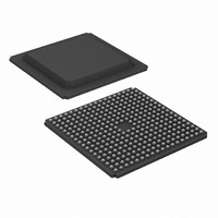
XC3S1500-5FGG320C Xilinx Inc, XC3S1500-5FGG320C Datasheet - Page 95

XC3S1500-5FGG320C
Manufacturer Part Number
XC3S1500-5FGG320C
Description
SPARTAN-3A FPGA 1.5M 320-FBGA
Manufacturer
Xilinx Inc
Series
Spartan™-3r
Datasheet
1.XC3S50-4VQG100C.pdf
(217 pages)
Specifications of XC3S1500-5FGG320C
Number Of Logic Elements/cells
29952
Number Of Labs/clbs
3328
Total Ram Bits
589824
Number Of I /o
221
Number Of Gates
1500000
Voltage - Supply
1.14 V ~ 1.26 V
Mounting Type
Surface Mount
Operating Temperature
0°C ~ 85°C
Package / Case
320-BGA
For Use With
NANO-SPARTAN - KIT NANOBOARD AND SPARTAN3 DC807-1001 - DAUGHTER CARD XILINX SPARTAN 3
Lead Free Status / RoHS Status
Lead free / RoHS Compliant
Available stocks
Company
Part Number
Manufacturer
Quantity
Price
Company:
Part Number:
XC3S1500-5FGG320C
Manufacturer:
XILINX
Quantity:
104
Company:
Part Number:
XC3S1500-5FGG320C
Manufacturer:
Xilinx Inc
Quantity:
10 000
- Current page: 95 of 217
- Download datasheet (6Mb)
Table 66: Timing for the Master and Slave Parallel Configuration Modes (Continued)
DS099-3 (v2.5) December 4, 2009
Product Specification
98
Notes:
1.
2.
3.
4.
Hold Times
T
T
T
Clock Timing
T
T
F
ΔF
SMCCD
SMCCCS
SMWCC
CCH
CCL
CCPAR
Symbol
CCPAR
The numbers in this table are based on the operating conditions set forth in
RDWR_B is synchronized to CCLK for the purpose of performing the Abort operation. The same pin asynchronously controls the
driver impedance of the D0 - D7 pins. To avoid contention when writing configuration data to the D0 - D7 bus, do not bring RDWR_B
High when CS_B is Low.
In the Slave Parallel mode, it is necessary to use the BUSY pin when the CCLK frequency exceeds this maximum specification.
Some Xilinx documents may refer to Parallel modes as "SelectMAP" modes.
(2)
R
The time from the rising transition at the CCLK pin to the point
when data is last held at the D0-D7 pins
The time from the rising transition at the CCLK pin to the point
when a logic level is last held at the CS_B pin
The time from the rising transition at the CCLK pin to the point
when a logic level is last held at the RDWR_B pin
CCLK input pin High pulse width
CCLK input pin Low pulse width
Frequency of the
clock signal at the
CCLK input pin
Variation from the CCLK output frequency set using the BitGen
option ConfigRate
No bitstream
compression
With bitstream compression
During STARTUP phase
Description
Spartan-3 FPGA Family: DC and Switching Characteristics
www.xilinx.com
Not using the BUSY pin
Using the BUSY pin
Table
31.
(3)
Master
Master
Slave/
Slave
Both
All Speed Grades
–50%
Min
0
0
0
5
0
0
0
5
0
+50%
Max
50
66
20
50
∞
∞
-
-
-
Units
MHz
MHz
MHz
MHz
ns
ns
ns
ns
ns
-
95
Related parts for XC3S1500-5FGG320C
Image
Part Number
Description
Manufacturer
Datasheet
Request
R

Part Number:
Description:
SPARTAN-3A FPGA 1.5M STD 676FBGA
Manufacturer:
Xilinx Inc
Datasheet:

Part Number:
Description:
FLASH
Manufacturer:
Xilinx Inc
Datasheet:

Part Number:
Description:
IC
Manufacturer:
Xilinx Inc
Datasheet:

Part Number:
Description:
FPGA Spartan®-3 Family 1.5M Gates 29952 Cells 630MHz 90nm Technology 1.2V 320-Pin FBGA
Manufacturer:
Xilinx Inc
Datasheet:

Part Number:
Description:
FPGA Spartan®-3 Family 1.5M Gates 29952 Cells 630MHz 90nm Technology 1.2V 320-Pin FBGA
Manufacturer:
Xilinx Inc
Datasheet:

Part Number:
Description:
FPGA Spartan®-3 Family 1.5M Gates 29952 Cells 630MHz 90nm Technology 1.2V 676-Pin FBGA
Manufacturer:
Xilinx Inc
Datasheet:

Part Number:
Description:
FPGA Spartan®-3 Family 1.5M Gates 29952 Cells 630MHz 90nm Technology 1.2V 676-Pin FBGA
Manufacturer:
Xilinx Inc
Datasheet:

Part Number:
Description:
FPGA Spartan®-3 Family 1.5M Gates 29952 Cells 725MHz 90nm Technology 1.2V 456-Pin FBGA
Manufacturer:
Xilinx Inc
Datasheet:

Part Number:
Description:
FPGA Spartan®-3 Family 1.5M Gates 29952 Cells 630MHz 90nm Technology 1.2V 456-Pin FBGA
Manufacturer:
Xilinx Inc
Datasheet:

Part Number:
Description:
FPGA Spartan®-3 Family 1.5M Gates 29952 Cells 725MHz 90nm Technology 1.2V 456-Pin FBGA
Manufacturer:
Xilinx Inc
Datasheet:

Part Number:
Description:
FPGA Spartan®-3 Family 1.5M Gates 29952 Cells 630MHz 90nm Technology 1.2V 676-Pin FBGA
Manufacturer:
Xilinx Inc
Datasheet:

Part Number:
Description:
SPARTAN-3A FPGA 1.5M STD 320FBGA
Manufacturer:
Xilinx Inc
Datasheet:

Part Number:
Description:
SPARTAN-3A FPGA 1.5M 676-FBGA
Manufacturer:
Xilinx Inc
Datasheet:

Part Number:
Description:
0974 AT END CALLS OUT FOR A SPECIFIC STEPPING CODE
Manufacturer:
Xilinx Inc

Part Number:
Description:
FPGA Spartan®-3 Family 1.5M Gates 29952 Cells 630MHz 90nm Technology 1.2V 320-Pin FBGA
Manufacturer:
Xilinx Inc
Datasheet:


