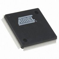
AT94K40AL-25DQU Atmel, AT94K40AL-25DQU Datasheet - Page 173

AT94K40AL-25DQU
Manufacturer Part Number
AT94K40AL-25DQU
Description
IC FPSLIC 40K GATE 25MHZ 208PQFP
Manufacturer
Atmel
Series
FPSLIC®r
Datasheet
1.AT94K05AL-25AJI.pdf
(204 pages)
Specifications of AT94K40AL-25DQU
Core Type
8-bit AVR
Speed
18MHz
Interface
I²C, UART
Program Sram Bytes
20K-32K
Fpga Sram
18kb
Data Sram Bytes
4K ~ 16K
Fpga Core Cells
2304
Fpga Gates
40K
Fpga Registers
2862
Voltage - Supply
3 V ~ 3.6 V
Mounting Type
Surface Mount
Operating Temperature
-40°C ~ 85°C
Package / Case
208-MQFP, 208-PQFP
For Use With
ATSTK594 - BOARD FPSLIC DAUGHTER FOR STK500
Lead Free Status / RoHS Status
Lead free / RoHS Compliant
Eeprom Size
-
Available stocks
Company
Part Number
Manufacturer
Quantity
Price
- Current page: 173 of 204
- Download datasheet (4Mb)
6.1
1138I–FPSLI–1/08
FPSLIC Dual-port SRAM Characteristics
The Dual-port SRAM operates in single-edge clock controlled mode during read operations, and
a double-edge controlled mode during write operations. Addresses are clocked internally on the
rising edge of the clock signal (ME). Any change of address without a rising edge of ME is not
considered.
In read mode, the rising clock edge triggers data read without any significant constraint on the
length of the clock pulse. The WE signal must be changed and held Low before the rising edge
of ME to signify a read cycle. The WE signal should then remain Low until the falling edge of the
clock.
In write mode, data applied to the inputs is latched on either the falling edge of WE or the falling
edge of the clock, whichever comes earlier, and written to memory. Also, WE must be High
before the rising edge of ME to signify a write cycle. If data inputs change during a write cycle,
only the value present at the write cycle end is considered and written to the address clocked at
the ME rise. A write cycle ending on WE fall does not turn into a read cycle – the next cycle will
be a read cycle if WE remains Low during rising edge of ME.
Figure 6-1.
Figure 6-2.
DATA READ
CLK (ME)
ADDR
DATA WRITE
WE
CLK (ME)
ADDR
WE
SRAM Read Cycle Timing Diagram
SRAM Write Cycle Timing Diagram
t
Previous Data
ADS
t
Address Valid
RDS
t
ADS
t
Address Valid
WRS
t
ADH
t
ACC
t
ADH
t
MEH
t
MPW
t
MPW
t
WDS
t
WDS
Data Valid
Output Valid
AT94KAL Series FPSLIC
t
t
t
RDH
MEL
WDH
t
WDH
t
t
t
t
t
t
t
ADS
ADH
RDS
RDH
ACC
MEH
MEL
t
t
t
t
t
t
ADS
ADH
WRS
MPW
WDS
WDH
- Address Setup
- Address Hold
- Read Cycle Setup
- Read Cycle Hold
- Access Time from posedge ME
- Minimum ME High
- Minimum ME Low
- Address Setup
- Address Hold
- Write Cycle Setup
- Minimum Write Duration
- Data Setup to Write End
- Data Hold to Write End
173
Related parts for AT94K40AL-25DQU
Image
Part Number
Description
Manufacturer
Datasheet
Request
R

Part Number:
Description:
IC FPSLIC 40K GATE 25MHZ 208PQFP
Manufacturer:
Atmel
Datasheet:

Part Number:
Description:
IC FPSLIC 40K GATE 25MHZ 144LQFP
Manufacturer:
Atmel
Datasheet:

Part Number:
Description:
IC FPSLIC 40K GATE 25MHZ 144LQFP
Manufacturer:
Atmel
Datasheet:

Part Number:
Description:
IC FPSLIC 40K GATE 25MHZ 144LQFP
Manufacturer:
Atmel
Datasheet:

Part Number:
Description:
At94kal Series Field Programmable System Level Integrated Circuit
Manufacturer:
ATMEL Corporation
Datasheet:

Part Number:
Description:
FPGA - Field Programmable Gate Array FPSLIC 40K GATE 8B AVR 25MHZ TEMP
Manufacturer:
Atmel

Part Number:
Description:
DEV KIT FOR AVR/AVR32
Manufacturer:
Atmel
Datasheet:

Part Number:
Description:
INTERVAL AND WIPE/WASH WIPER CONTROL IC WITH DELAY
Manufacturer:
ATMEL Corporation
Datasheet:

Part Number:
Description:
Low-Voltage Voice-Switched IC for Hands-Free Operation
Manufacturer:
ATMEL Corporation
Datasheet:

Part Number:
Description:
MONOLITHIC INTEGRATED FEATUREPHONE CIRCUIT
Manufacturer:
ATMEL Corporation
Datasheet:

Part Number:
Description:
AM-FM Receiver IC U4255BM-M
Manufacturer:
ATMEL Corporation
Datasheet:

Part Number:
Description:
Monolithic Integrated Feature Phone Circuit
Manufacturer:
ATMEL Corporation
Datasheet:

Part Number:
Description:
Multistandard Video-IF and Quasi Parallel Sound Processing
Manufacturer:
ATMEL Corporation
Datasheet:


