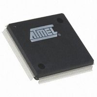
AT94K40AL-25DQU Atmel, AT94K40AL-25DQU Datasheet - Page 54

AT94K40AL-25DQU
Manufacturer Part Number
AT94K40AL-25DQU
Description
IC FPSLIC 40K GATE 25MHZ 208PQFP
Manufacturer
Atmel
Series
FPSLIC®r
Datasheet
1.AT94K05AL-25AJI.pdf
(204 pages)
Specifications of AT94K40AL-25DQU
Core Type
8-bit AVR
Speed
18MHz
Interface
I²C, UART
Program Sram Bytes
20K-32K
Fpga Sram
18kb
Data Sram Bytes
4K ~ 16K
Fpga Core Cells
2304
Fpga Gates
40K
Fpga Registers
2862
Voltage - Supply
3 V ~ 3.6 V
Mounting Type
Surface Mount
Operating Temperature
-40°C ~ 85°C
Package / Case
208-MQFP, 208-PQFP
For Use With
ATSTK594 - BOARD FPSLIC DAUGHTER FOR STK500
Lead Free Status / RoHS Status
Lead free / RoHS Compliant
Eeprom Size
-
Available stocks
Company
Part Number
Manufacturer
Quantity
Price
- Current page: 54 of 204
- Download datasheet (4Mb)
4.13
54
FPGA Cache Logic
AT94KAL Series FPSLIC
• Bit 0 - EXTRF: External (Software) Reset Flag
This flag is set (one) in three separate circumstances: power-on reset, use of Resetn/AVRRe-
setn and writing a one to the SRST bit in the Software Control Register – SFTCR. The PORF
flag can be checked to eliminate power-on reset as a cause for this flag to be set. There is no
way to differentiate between use of Resetn/AVRResetn and software reset. The flag can only be
cleared (zero) by writing a zero to the EXTRF bit. The bit will not be cleared by the hardware dur-
ing AVR reset.
Table 4-3.
FPGA Cache Data Register – FPGAD
The FPGAD I/O Register address is not supported by a physical register; it is simply the I/O
address that, if written to, generates the FPGA Cache I/O write strobe. The CACHEIOWE signal
is a qualified version of the AVR IOWE signal. It will only be active if an OUT or ST (store to)
instruction references the FPGAD I/O address. The FPGAD I/O address is write-sensitive-only;
an I/O read to this location is ignored. If the AVR Cache Interface bit in the SCR [BIT62] is set
(one), the data being “written” to this address is cached to the FPGA address specified by the
FPGAX..Z registers (see below) during the active CACHEIOWE strobe.
FPGA Cache Z Address Registers – FPGAX..Z
The three FPGA Cache address registers combine to form the 24-bit address, CAC-
HEADDR[23:0], delivered to the FPGA cache logic outside the AVR block during a write to the
FPGAD I/O Register (see above).
Bit
$1B ($3B)
Read/Write
Initial Value
Bit
$18 ($38)
$19 ($39)
$1A ($3A)
Read/Write
Initial Value
SM1
Sleep Mode Select
0
0
1
1
7
MSB
W
N/A
7
FCX7
FCY7
FCT3
R/W
0
N/A
6
W
6
FCX6
FCY6
FCT2
R/W
0
5
W
N/A
5
FCX5
FCY5
FCT1
R/W
0
4
W
N/A
R/W
4
FCX4
FCY4
FCT0
0
SM0
0
1
0
1
3
W
N/A
3
FCX3
FCY3
FCZ3
R/W
0
2
W
N/A
2
FCX2
FCY2
FCZ2
R/W
0
Sleep Mode
Idle
Reserved
Power-down
Power-save
1
W
N/A
1
FCX1
FCY1
FCZ1
R/W
0
0
LSB
W
N/A
0
FCX0
FCY0
FCZ0
R/W
0
1138I–FPSLI–1/08
FPGAD
FPGAX
FPGAY
FPGAZ
Related parts for AT94K40AL-25DQU
Image
Part Number
Description
Manufacturer
Datasheet
Request
R

Part Number:
Description:
IC FPSLIC 40K GATE 25MHZ 208PQFP
Manufacturer:
Atmel
Datasheet:

Part Number:
Description:
IC FPSLIC 40K GATE 25MHZ 144LQFP
Manufacturer:
Atmel
Datasheet:

Part Number:
Description:
IC FPSLIC 40K GATE 25MHZ 144LQFP
Manufacturer:
Atmel
Datasheet:

Part Number:
Description:
IC FPSLIC 40K GATE 25MHZ 144LQFP
Manufacturer:
Atmel
Datasheet:

Part Number:
Description:
At94kal Series Field Programmable System Level Integrated Circuit
Manufacturer:
ATMEL Corporation
Datasheet:

Part Number:
Description:
FPGA - Field Programmable Gate Array FPSLIC 40K GATE 8B AVR 25MHZ TEMP
Manufacturer:
Atmel

Part Number:
Description:
DEV KIT FOR AVR/AVR32
Manufacturer:
Atmel
Datasheet:

Part Number:
Description:
INTERVAL AND WIPE/WASH WIPER CONTROL IC WITH DELAY
Manufacturer:
ATMEL Corporation
Datasheet:

Part Number:
Description:
Low-Voltage Voice-Switched IC for Hands-Free Operation
Manufacturer:
ATMEL Corporation
Datasheet:

Part Number:
Description:
MONOLITHIC INTEGRATED FEATUREPHONE CIRCUIT
Manufacturer:
ATMEL Corporation
Datasheet:

Part Number:
Description:
AM-FM Receiver IC U4255BM-M
Manufacturer:
ATMEL Corporation
Datasheet:

Part Number:
Description:
Monolithic Integrated Feature Phone Circuit
Manufacturer:
ATMEL Corporation
Datasheet:

Part Number:
Description:
Multistandard Video-IF and Quasi Parallel Sound Processing
Manufacturer:
ATMEL Corporation
Datasheet:


