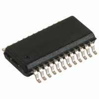
CY7C63101C-QXC Cypress Semiconductor Corp, CY7C63101C-QXC Datasheet - Page 16

CY7C63101C-QXC
Manufacturer Part Number
CY7C63101C-QXC
Description
IC MCU 4K USB MCU LS 24QSOP
Manufacturer
Cypress Semiconductor Corp
Series
M8™r
Datasheet
1.CY7C63101C-QXC.pdf
(28 pages)
Specifications of CY7C63101C-QXC
Applications
USB Microcontroller
Core Processor
M8A
Program Memory Type
OTP (4 kB)
Controller Series
CY7C631xx
Ram Size
128 x 8
Interface
USB
Number Of I /o
16
Voltage - Supply
4 V ~ 5.25 V
Operating Temperature
0°C ~ 70°C
Mounting Type
Surface Mount
Package / Case
24-QSOP
Lead Free Status / RoHS Status
Lead free / RoHS Compliant
Other names
428-1851
Document #: 38-08026 Rev. *B
Bits 0 to 3 indicate the numbers of data bytes to be transmitted
during an IN packet, valid values are 0 to 8 inclusive.
Bit 4 must be set before Endpoint 1 can be used. If this bit is
cleared, the USB Controller ignores all traffic to Endpoint 1.
Setting the Stall bit (bit 5) stalls IN and OUT packets until this
bit is cleared.
Bit 6 (Data 1/0) must be set to either 0 or 1 depending on the
data packet’s toggle state, 0 for DATA0, 1 for DATA1.
After the transmit data has been loaded into the FIFO, bit 6
should be set according to the data toggle state and bit 7 set
to “1”. This enables the USB Controller to respond to an IN
packet. Bit 7 is cleared and an Endpoint 1 interrupt is
generated by the SIE once the host acknowledges the data
transmission.
6.9.4
USB status and control is regulated by USB Status and Control
Register located at I/O address 0x13 as shown in Figure 6-21.
This is a read/write register. All reserved bits must be written
to zero. All bits in the register are cleared during reset.
Bit 0 is set by the SIE if any USB activity except idle (D+ LOW,
D– HIGH) is detected. The user program should check and
clear this bit periodically to detect any loss of bus activity.
Reserved
b7
0
USB Status and Control
Reserved
b6
0
Figure 6-21. USB Status and Control Register (USB SCR - Address 0x13)
Reserved
b5
0
ENOUTS
R/W
b4
0
STATOUTS
Writing a 0 to this bit clears it. Writing a 1 does not change its
value.
Bit 1 is used to force the on-chip USB transmitter to the K state
which sends a Resume signal to the host. Bit 2 is used to force
the transmitter to the J state. This bit should normally be set to
zero. However, for resume signaling, force a J state for one
instruction before forcing resume.
Bit 3 is used to automatically respond to the Status stage OUT
of a control read transfer on Endpoint 0. A valid Status stage
OUT contains a DATA1 packet with 0 bytes of data. If the Statu-
sOuts bit is set, the USB engine responds to a valid Status
stage OUT with an ACK, and any other OUT with a STALL.
The data is not written into the FIFO when this bit is set. This
bit is cleared when a SETUP token is received by Endpoint 0.
Bit 4 is used to enable the receiving of Endpoint 0 OUT
packets. When this bit is set to 1, the data from an OUT trans-
action is written into the Endpoint 0 FIFO. If this bit is 0, data
is not written to the FIFO and the SIE responds with a NAK.
This bit is cleared following a SETUP or ACKed OUT trans-
action. Note: After firmware decodes a SETUP packet and
prepares for a subsequent OUT transaction by setting bit 4, bit
4 is not cleared until the hand-shake phase of an ACKed OUT
transaction (a NAKed OUT transaction does not clear this bit).
R/W
b3
0
FORCEJ
b2
0
FORCEK
R/W
b1
0
CY7C63001C
CY7C63101C
Page 16 of 28
BUSACT
R/W
b0
0


