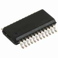
CY7C63101C-QXC Cypress Semiconductor Corp, CY7C63101C-QXC Datasheet - Page 3

CY7C63101C-QXC
Manufacturer Part Number
CY7C63101C-QXC
Description
IC MCU 4K USB MCU LS 24QSOP
Manufacturer
Cypress Semiconductor Corp
Series
M8™r
Datasheet
1.CY7C63101C-QXC.pdf
(28 pages)
Specifications of CY7C63101C-QXC
Applications
USB Microcontroller
Core Processor
M8A
Program Memory Type
OTP (4 kB)
Controller Series
CY7C631xx
Ram Size
128 x 8
Interface
USB
Number Of I /o
16
Voltage - Supply
4 V ~ 5.25 V
Operating Temperature
0°C ~ 70°C
Mounting Type
Surface Mount
Package / Case
24-QSOP
Lead Free Status / RoHS Status
Lead free / RoHS Compliant
Other names
428-1851
Document #: 38-08026 Rev. *B
4.0
5.0
6.0
The Cypress CY7C630/101C USB microcontrollers are
optimized for human-interface computer peripherals such as
a mouse, joystick, and gamepad. These USB microcontrollers
conform to the low-speed (1.5 Mbps) requirements of the USB
specification
self-contained unit with: a USB interface engine, USB trans-
ceivers, an 8-bit RISC microcontroller, a clock oscillator,
timers, and program memory. Each microcontroller supports
one USB device address and two endpoints.
The 6-MHz clock is doubled to 12 MHz to drive the microcon-
troller. A RISC architecture with 35 instructions provides the
best balance between performance and product cost.
6.1
The memory in the USB Controller is organized into user
program memory in EPROM space and data memory in SRAM
space.
V
V
V
XTALIN
XTALOUT
P0.0–P0.7,
P1.0–P1.7
D+, D–
CEXT
Name
CEXT
D+
D–
V
V
V
CC
SS
PP
PP
CC
SS
Name
Memory Organization
Pin Definitions
Pin Description
Functional Description
version
I/O
I/O
I/O
I/O
1 pin. Connects to the USB power source or to a nominal 5V power supply. Actual V
between 4.0V and 5.25V.
1 pin. Connects to ground.
1 pin. Used in programming the on-chip EPROM. This pin should be tied to ground during normal operations.
1 pin. Input from an external ceramic resonator.
1 pin. Return path for the ceramic resonator (leave unconnected if driving XTALIN from an external oscillator).
16 pins. P0.0–P0.7 are the 8 I/O lines in Port 0. P1.0–P1.7 are the 8 I/O lines in Port 1. P1.0–P1.3 are
supported in the CY7C63001C. All I/O pins include bit-programmable pull-up resistors. However, the sink
current of each pin can be programmed to one of sixteen levels. Besides functioning as GPIO lines, each
pin can be programmed as an interrupt input. The interrupt is edge-triggered, with programmable polarity.
2 pins. Bidirectional USB data lines. An external pull-up resistor must be connected between the D pin and
V
1 pin. Open-drain output with Schmitt trigger input. The input is connected to a rising edge-triggered interrupt.
CEXT may be connected to an external RC to generate a wake-up from Suspend mode. See Section 6.4.
–
–
–
CC
1.1.
to select low-speed USB operation.
20-Pin
(continued)
Each
14
13
12
9
8
7
microcontroller
24-pin
16
15
10
14
11
9
is
Die Pad #
a
11
16
15
10
14
9
6.1.1
The CY7C63001C and CY7C63101C each offer 4 Kbytes of
EPROM. The program memory space is divided into two
functional groups: interrupt vectors and program code.
The interrupt vectors occupy the first 16 bytes of the program
space. Each vector is 2 bytes long. After a reset, the Program
Counter points to location zero of the program space.
Figure 6-1 shows the organization of the Program Memory
Space.
6.1.2
The Cypress USB microcontroller includes a security fuse bit.
When the security fuse is programmed, the EPROM program
memory outputs 0xFF to the EPROM programmer, thus
protecting the user’s code.
Description
Description
Connects to external R/C timing circuit for optional
‘suspend’ wakeup
USB data+
USB data–
Programming voltage supply, tie to ground during normal
operation
Voltage supply
Ground
Program Memory Organization
Security Fuse Bit
CY7C63001C
CY7C63101C
CC
range can vary
Page 3 of 28


