CY7C63101C-QXC Cypress Semiconductor Corp, CY7C63101C-QXC Datasheet - Page 6
CY7C63101C-QXC
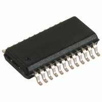
Manufacturer Part Number
CY7C63101C-QXC
Description
IC MCU 4K USB MCU LS 24QSOP
Manufacturer
Cypress Semiconductor Corp
Series
M8™r
Datasheet
1.CY7C63101C-QXC.pdf
(28 pages)
Specifications of CY7C63101C-QXC
Applications
USB Microcontroller
Core Processor
M8A
Program Memory Type
OTP (4 kB)
Controller Series
CY7C631xx
Ram Size
128 x 8
Interface
USB
Number Of I /o
16
Voltage - Supply
4 V ~ 5.25 V
Operating Temperature
0°C ~ 70°C
Mounting Type
Surface Mount
Package / Case
24-QSOP
Lead Free Status / RoHS Status
Lead free / RoHS Compliant
Other names
428-1851


Document #: 38-08026 Rev. *B
6.2
I/O registers are accessed via the I/O Read (IORD) and I/O
Write (IOWR, IOWX) instructions.
Table 6-1. I/O Register Summary
6.3
The USB Controller supports three types of resets. All
registers are restored to their default states during a reset. The
USB Device Address is set to 0 and all interrupts are disabled.
In addition, the Program Stack Pointer (PSP) is set to 0x00 and
the Data Stack Pointer (DSP) is set to 0x00. The user should
set the DSP to a location such as 0x70 to reserve 16 bytes of
USB FIFO space. The assembly instructions to do so are:
The three reset types are:
The occurrence of a reset is recorded in the Status and Control
Register located at I/O address 0xFF (Figure 6-3). Reading
1. Power-On Reset (POR)
2. Watch Dog Reset (WDR)
3. USB Reset
P0 Data
P1 Data
P0 IE
P1 IE
P0 Pull-up
P1 Pull-up
EP0 TX Config.
EP1 TX Config.
USB DA
USB SCR
EP0 RX Status
GIE
WDT
Cext
Timer
P0 Isink
P1 Isink
SCR
MOV A, 70h
instead of 6F because the dsp is
data transfer of the PUSH instruction occurs
SWAP A, DSP
Register Name
I/O Register Summary
Reset
; Move 70 hex into Accumulator, use 70
; always decremented by 1 before the
; Move Accumulator value into dsp
I/O Address
0x30-0x37
0x38-0x3F
0xFF
0x00
0x01
0x04
0x05
0x08
0x09
0x10
0x11
0x12
0x13
0x14
0x20
0x21
0x22
0x23
Read/Write
R/W
R/W
R/W
R/W
R/W
R/W
R/W
R/W
R/W
R/W
W
W
W
W
W
W
W
R
General purpose I/O Port (low current)
General purpose I/O Port (high current)
Interrupt enable for Port 0 pins
Interrupt enable for Port 1 pins
Pull-up resistor control for Port 0 pins
Pull-up resistor control for Port 1 pins
USB Endpoint 0 transmit configuration
USB Endpoint 1 transmit configuration
USB device address
USB status and control
USB Endpoint 0 receive status
Global Interrupt Enable
Watch Dog Timer clear
External R-C Timing circuit control
Free-running timer
Input sink current control for Port 0 pins. There is
one Isink register for each pin. Address of the Isink
register for pin 0 is located at 0x30 and the register
address for pin 7 is located at 0x37.
Input sink current control for Port 1 pins. There is
one Isink register for each pin. Address of the Isink
register for pin 0 is located at 0x38 and the register
address for pin 7 is located at 0x3F. The number
of Port 1 pins depends on package type.
Processor status and control register
and writing this register are supported by the IORD and IOWR
instructions. Bits 1, 2, and 7 are reserved and must be written
as zeros during a write. During a read, reserved bit positions
should be ignored. Bits 4, 5, and 6 are used to record the
occurrence of POR, USB, and WDR Reset respectively. The
firmware can interrogate these bits to determine the cause of
a reset. If a Watch Dog Reset occurs, firmware must clear the
WDR bit (bit 6) in the Status and Control Register to re-enable
the USB transmitter (please refer to the Watch Dog Reset
section for further details). Bit 0, the “Run” control, is set to 1
at POR. Clearing this bit stops the microcontroller (firmware
normally should not clear this bit). Once this bit is set to LOW,
only a reset can set this bit HIGH.
The microcontroller resumes execution from ROM address
0x00 after a reset unless the Suspend bit (bit 3) of the Status
and Control Register is set. Setting the Suspend bit stops the
clock oscillator and the interrupt timers and powers down the
microcontroller. The detection of any USB activity, the occur-
rence of a GPIO Interrupt, or the occurrence of the Cext
Interrupt terminates the suspend condition.
Function
CY7C63001C
CY7C63101C
Page 6 of 28
Page
12
12
10
10
15
15
14
16
14
11
10
10
9
9
7
8
8
7
Related parts for CY7C63101C-QXC
Image
Part Number
Description
Manufacturer
Datasheet
Request
R

Part Number:
Description:
Manufacturer:
Cypress Semiconductor Corp
Datasheet:
Part Number:
Description:
Manufacturer:
Cypress Semiconductor Corp
Datasheet:
Part Number:
Description:
Manufacturer:
Cypress Semiconductor Corp
Datasheet:
Part Number:
Description:
Manufacturer:
Cypress Semiconductor Corp
Datasheet:
Part Number:
Description:
Manufacturer:
Cypress Semiconductor Corp
Datasheet: