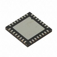
CY8CTMG201-32LQXI Cypress Semiconductor Corp, CY8CTMG201-32LQXI Datasheet - Page 151

CY8CTMG201-32LQXI
Manufacturer Part Number
CY8CTMG201-32LQXI
Description
IC MCU 16K FLASH PSOC 32UQFN
Manufacturer
Cypress Semiconductor Corp
Series
TrueTouch™r
Datasheet
1.CY8CTST200-16LGXI.pdf
(308 pages)
Specifications of CY8CTMG201-32LQXI
Applications
Touchscreen Controller
Core Processor
M8C
Program Memory Type
FLASH (16 kB)
Controller Series
CY8CT
Ram Size
2K x 8
Interface
I²C, SPI, UART/USART, USB
Number Of I /o
28
Voltage - Supply
1.8 V
Operating Temperature
-40°C ~ 85°C
Mounting Type
Surface Mount
Package / Case
32-UQFN Exposed Pad, 32-HUQFN, 32-SQFN
Processor Series
CY8CTxx2xx
Core
M8C
For Use With
770-1000 - ISP 4PORT FOR CYPRESS PSOC MCU
Lead Free Status / RoHS Status
Lead free / RoHS Compliant
Other names
428-2971
- Current page: 151 of 308
- Download datasheet (3Mb)
18.3
18.3.1
Figure 18-3
as 0, 1, 2, or 3. These mode numbers are an encoding of
two control bits: Clock Phase and Clock Polarity.
Clock Phase indicates the relationship of the clock to the
data. When the clock phase is '0', it means that the data is
registered as an input on the leading edge of the clock and
the next data is output on the trailing edge of the clock.
When the clock phase is '1', it means that the next data is
output on the leading edge of the clock and that data is reg-
istered as an input on the trailing edge of the clock.
Clock Polarity controls clock inversion. When clock polarity
is set to '1’, the clock idle state is high.
PSoC CY8CTMG20x and CY8CTST200 TRM, Document No. 001-53603 Rev. *C
Timing Diagrams
shows the SPI modes that are typically defined
SCLK, Polarity=0 (Mode 0)
SCLK, Polarity=1 (Mode 1)
SCLK, Polarity=0 (Mode 2)
SCLK, Polarity=1 (Mode 3)
SPI Mode Timing
MISO
MISO
MOSI
MOSI
SS_
SS_
MODE 0, 1 (Phase=0) Input on leading edge. Output on trailing edge.
MODE 2, 3 (Phase=1) Output on leading edge. Input on trailing edge.
Figure 18-3. SPI Mode Timing
7
7
6
6
5
5
4
4
3
3
2
2
1
1
0
0
151
SPI
[+] Feedback
Related parts for CY8CTMG201-32LQXI
Image
Part Number
Description
Manufacturer
Datasheet
Request
R
Part Number:
Description:
IC MCU 16K FLASH PSOC 48-QFN
Manufacturer:
Cypress Semiconductor Corp
Datasheet:
Part Number:
Description:
IC MCU 16K FLASH PSOC 32UQFN
Manufacturer:
Cypress Semiconductor Corp
Part Number:
Description:
IC MCU 16K FLASH PSOC 48-QFN
Manufacturer:
Cypress Semiconductor Corp
Part Number:
Description:
Manufacturer:
Cypress Semiconductor Corp
Datasheet:
Part Number:
Description:
Manufacturer:
Cypress Semiconductor Corp
Datasheet:
Part Number:
Description:
Manufacturer:
Cypress Semiconductor Corp
Datasheet:
Part Number:
Description:
Manufacturer:
Cypress Semiconductor Corp
Datasheet:


