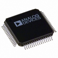
ADE7166ASTZF16 Analog Devices Inc, ADE7166ASTZF16 Datasheet - Page 108

ADE7166ASTZF16
Manufacturer Part Number
ADE7166ASTZF16
Description
IC ENERGY METER 1PHASE 64LQFP
Manufacturer
Analog Devices Inc
Specifications of ADE7166ASTZF16
Applications
Energy Measurement
Core Processor
8052
Program Memory Type
FLASH (16 kB)
Controller Series
ADE71xx
Ram Size
512 x 8
Interface
I²C, SPI, UART
Number Of I /o
20
Voltage - Supply
3.135 V ~ 3.465 V
Operating Temperature
-40°C ~ 85°C
Mounting Type
Surface Mount
Package / Case
64-LQFP
Ic Function
Single Phase Energy Measurement IC
Supply Voltage Range
3.13V To 3.46V, 2.4V To 3.7V
Operating Temperature Range
-40°C To +85°C
Digital Ic Case Style
LQFP
No. Of Pins
64
Lead Free Status / RoHS Status
Lead free / RoHS Compliant
Lead Free Status / RoHS Status
Lead free / RoHS Compliant, Lead free / RoHS Compliant
Available stocks
Company
Part Number
Manufacturer
Quantity
Price
Company:
Part Number:
ADE7166ASTZF16
Manufacturer:
VHK
Quantity:
2
Company:
Part Number:
ADE7166ASTZF16
Manufacturer:
Analog Devices Inc
Quantity:
10 000
Company:
Part Number:
ADE7166ASTZF16-RL
Manufacturer:
KOA
Quantity:
50 000
Company:
Part Number:
ADE7166ASTZF16-RL
Manufacturer:
Analog Devices Inc
Quantity:
10 000
ADE7116/ADE7156/ADE7166/ADE7169/ADE7566/ADE7569
FLASH MEMORY
FLASH MEMORY OVERVIEW
Flash memory is a type of nonvolatile memory that is in-circuit
programmable. The default, erased state of a byte of flash memory
is 0xFF. When a byte of flash memory is programmed, the required
bits change from 1 to 0. The flash memory must be erased to
turn the 0s back to 1s. A byte of flash memory cannot, however,
be erased individually. The entire segment, or page, of flash
memory that contains the byte must be erased.
The ADE7116/ADE7156/ADE7166/ADE7169/ADE7566/
ADE7569 provide 16 kB of flash program/information memory.
This memory is segmented into 32 pages that each contain 512
bytes each. To reprogram one byte of flash memory, the other
511 bytes in that page must be erased. The flash memory can be
erased by page or all at once in a mass erase. There is a command
to verify that a flash write operation has completed successfully.
The ADE7116/ADE7156/ADE7166/ADE7169/ADE7566/
ADE7569 flash memory controller also offers configurable flash
memory protection.
The 16 kB of flash memory are provided on-chip to facilitate
code execution without any external discrete ROM device
requirements. The program memory can be programmed in-
circuit, using the serial download mode provided or using
conventional third party memory programmers.
Flash/EE Memory Reliability
The flash memory arrays on the ADE7116/ADE7156/
ADE7166/ADE7169/ADE7566/ADE7569 are fully qualified for
two key Flash/EE memory characteristics: Flash/EE memory
cycling endurance and Flash/EE memory data retention.
Endurance quantifies the ability of the Flash/EE memory to be
cycled through many program, read, and erase cycles. In real
terms, a single endurance cycle is composed of four independent,
sequential events:
1.
2.
3.
4.
Initial page erase sequence.
Read/verify sequence.
Byte program sequence.
Second read/verify sequence.
Rev. B | Page 108 of 152
In reliability qualification, every byte in both the program and
data Flash/EE memory is cycled from 0x00 to 0xFF until a first
fail is recorded, signifying the endurance limit of the on-chip
Flash/EE memory.
As indicated in the Specifications section, the ADE7116/
ADE7156/ADE7166/ADE7169/ADE7566/ADE7569 flash
memory endurance qualification has been carried out in
accordance with JEDEC Standard 22 Method A117 over the
industrial temperature range of −40°C, +25°C, and +85°C. The
results allow the specification of a minimum endurance figure
over supply and temperature of 100,000 cycles, with a minimum
endurance figure of 20,000 cycles of operation at 25°C.
Retention is the ability of the flash memory to retain its
programmed data over time. Again, the parts have been
qualified in accordance with the formal JEDEC Retention
Lifetime Specification (A117) at a specific junction temperature
(T
As part of this qualification procedure, the flash memory is
cycled to its specified endurance limit described previously,
before data retention is characterized. This means that the flash
memory is guaranteed to retain its data for its full specified
retention lifetime every time the flash memory is
reprogrammed. It should also be noted that retention lifetime,
based on an activation energy of 0.6 eV, derates with T
shown in Figure 93.
J
= 55°C).
300
250
200
150
100
50
0
40
Figure 93. Flash/EE Memory Data Retention
50
T
J
60
JUNCTION TEMPERATURE (°C)
ANALOG DEVICES
100 YEARS MIN.
SPECIFICATION
AT T
70
J
= 55 ° C
80
90
100
J
as
110


