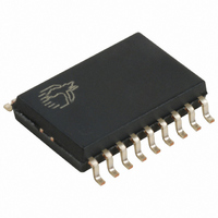
CY7C63231A-SC Cypress Semiconductor Corp, CY7C63231A-SC Datasheet - Page 23

CY7C63231A-SC
Manufacturer Part Number
CY7C63231A-SC
Description
IC MCU 3K USB LS PERIPH 18-SOIC
Manufacturer
Cypress Semiconductor Corp
Series
enCoRe™r
Datasheet
1.CY7C63231A-SXC.pdf
(50 pages)
Specifications of CY7C63231A-SC
Applications
USB Microcontroller
Core Processor
M8B
Program Memory Type
OTP (3 kB)
Controller Series
CY7C632xx
Ram Size
96 x 8
Interface
USB
Number Of I /o
10
Voltage - Supply
3.5 V ~ 5.5 V
Operating Temperature
0°C ~ 70°C
Mounting Type
Surface Mount
Package / Case
18-SOIC (7.5mm Width)
Operating Temperature (max)
70C
Operating Temperature (min)
0C
Operating Temperature Classification
Commercial
Package Type
SOIC
Mounting
Surface Mount
Lead Free Status / RoHS Status
Contains lead / RoHS non-compliant
Other names
428-1317
Available stocks
Company
Part Number
Manufacturer
Quantity
Price
Part Number:
CY7C63231A-SC
Manufacturer:
CYP
Quantity:
20 000
13.1
A typical USB enumeration sequence is shown below. In this description, ‘Firmware’ refers to embedded firmware in the
controller.
10.Once the device receives a Set Configuration request, its functions may now be used.
13.2
USB status and control is regulated by the USB Status and Control Register as shown in Figure 13-1.
Bit 7: PS/2 Pull-up Enable
Bit 6: VREG Enable
Bit 5: USB-PS/2 Interrupt Select
Bit 4: Reserved. Must be written as a ‘0’.
Document #: 38-08028 Rev. *B
11.Firmware should take appropriate action for Endpoint 1 transactions, which may occur from this point.
1. The host computer sends a SETUP packet followed by a DATA packet to USB address 0 requesting the Device descriptor.
2. Firmware decodes the request and retrieves its Device descriptor from the program memory tables.
3. The host computer performs a control read sequence and Firmware responds by sending the Device descriptor over the USB
4. After receiving the descriptor, the host sends a SETUP packet followed by a DATA packet to address 0 assigning a new USB
5. Firmware stores the new address in its USB Device Address Register after the no-data control sequence completes.
6. The host sends a request for the Device descriptor using the new USB address.
7. Firmware decodes the request and retrieves the Device descriptor from program memory tables.
8. The host performs a control read sequence and Firmware responds by sending its Device descriptor over the USB bus.
9. The host generates control reads from the device to request the Configuration and Report descriptors.
Read/Write
Bit Name
bus, via the on-chip FIFO.
address to the device.
This bit is used to enable the internal PS/2 pull-up resistors on the SDATA and SCLK pins. Normally the output high level on
these pins is V
or if the Device Address is enabled (bit 7 of the USB Device Address Register, Figure 14-1).
1 = Enable PS/2 pull-up resistors. The SDATA and SCLK pins are pulled up internally to V
5 kΩ (see Section 23.0 for the value of R
0 = Disable PS/2 pull-up resistors.
A 3.3V voltage regulator is integrated on chip to provide a voltage source for a 1.5-kΩ pull-up resistor connected to the D– pin
as required by the USB Specification. Note that the VREG output has an internal series resistance of approximately 200Ω, the
external pull-up resistor required is approximately 1.3-kΩ (see Figure 16-1).
1 = Enable the 3.3V output voltage on the VREG pin.
0 = Disable. The VREG pin can be configured as an input.
This bit allows the user to select whether an USB bus reset interrupt or a PS/2 activity interrupt will be generated when the
interrupt conditions are detected.
1 = PS/2 interrupt mode. A PS/2 activity interrupt will occur if the SDATA pin is continuously LOW for 128 to 256 µs.
0 = USB interrupt mode (default state). In this mode, a USB bus reset interrupt will occur if the single ended zero (SE0, D–
and D+ are LOW) exists for 128 to 256 µs.
See Section 19.0 for more details.
Reset
Bit #
USB Enumeration
USB Port Status and Control
PS/2 Pull-up
Enable
CC
R/W
, but note that the output will be clamped to approximately 1 Volt above V
7
0
Figure 13-1. USB Status and Control Register (Address 0x1F)
Enable
VREG
R/W
6
0
FOR
FOR
PS/2 Activity
USB Reset-
PS2
Interrupt
Mode
R/W
).
5
0
Reserved
4
0
-
Bus Activity
USB
R/W
3
0
R/W
CC
2
0
with two resistors of approximately
REG
CY7C63221/31A
enCoRe™ USB
D+/D- Forcing Bit
if the VREG Enable bit is set,
R/W
1
0
Page 23 of 50
R/W
0
0
[+] Feedback


