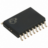
CY7C63231A-SC Cypress Semiconductor Corp, CY7C63231A-SC Datasheet - Page 6

CY7C63231A-SC
Manufacturer Part Number
CY7C63231A-SC
Description
IC MCU 3K USB LS PERIPH 18-SOIC
Manufacturer
Cypress Semiconductor Corp
Series
enCoRe™r
Datasheet
1.CY7C63231A-SXC.pdf
(50 pages)
Specifications of CY7C63231A-SC
Applications
USB Microcontroller
Core Processor
M8B
Program Memory Type
OTP (3 kB)
Controller Series
CY7C632xx
Ram Size
96 x 8
Interface
USB
Number Of I /o
10
Voltage - Supply
3.5 V ~ 5.5 V
Operating Temperature
0°C ~ 70°C
Mounting Type
Surface Mount
Package / Case
18-SOIC (7.5mm Width)
Operating Temperature (max)
70C
Operating Temperature (min)
0C
Operating Temperature Classification
Commercial
Package Type
SOIC
Mounting
Surface Mount
Lead Free Status / RoHS Status
Contains lead / RoHS non-compliant
Other names
428-1317
Available stocks
Company
Part Number
Manufacturer
Quantity
Price
Part Number:
CY7C63231A-SC
Manufacturer:
CYP
Quantity:
20 000
2.0
2.1
Cypress has reinvented its leadership position in the low-speed USB market with a new family of innovative microcontrollers.
Introducing...enCoRe™ USB—“enhanced Component Reduction.” Cypress has leveraged its design expertise in USB solutions
to create a new family of low-speed USB microcontrollers that enables peripheral developers to design new products with a
minimum number of components. At the heart of the Cypress enCoRe USB technology is the breakthrough design of a crystal-
less oscillator. By integrating the oscillator into the chip, an external crystal or resonator is no longer needed. We have also
integrated other external components commonly found in low-speed USB applications such as pull-up resistors, wake-up circuitry,
and a 3.3V regulator. All of this adds up to a lower system cost.
The family is comprised of 8-bit RISC One Time Programmable (OTP) microcontrollers. The instruction set has been optimized
specifically for USB and PS/2 operations, although the microcontrollers can be used for a variety of other embedded applications.
The features up to 10 general-purpose I/O (GPIO) pins to support USB, PS/2 and other applications. The I/O pins are grouped
into two ports (Port 0 to 1) where each pin can be individually configured as inputs with internal pull-ups, open drain outputs, or
traditional CMOS outputs with programmable drive strength of up to 50 mA output drive. Additionally, each I/O pin can be used
to generate a GPIO interrupt to the microcontroller.
The microcontrollers feature an internal oscillator. With the presence of USB traffic, the internal oscillator can be set to precisely
tune to USB timing requirements (6 MHz ±1.5%). This clock generator has been optimized to reduce clock-related noise
emissions (EMI), and provides the 6-MHz and 12-MHz clocks that remain internal to the microcontroller. When using the internal
oscillator, XTALIN and XTALOUT can be configured as additional input pins that can be read on port 2. Optionally, an external 6-
MHz ceramic resonator can be used to provide a higher precision reference if needed.
The is offered with 3 Kbytes of EPROM to minimize cost, and has 96 bytes of data RAM for stack space, user variables, and
USB endpoint FIFOs.
The family includes low-voltage reset logic, a watchdog timer, a vectored interrupt controller, and a 12-bit free-running timer. The
low-voltage reset (LVR) logic detects when power is applied to the device, resets the logic to a known state, and begins executing
instructions at EPROM address 0x0000. LVR will also reset the part when V
watchdog timer can be used to ensure the firmware never gets stalled for more than approximately 8 ms.
The microcontroller supports 7 maskable interrupts in the vectored interrupt controller. Interrupt sources include the USB Bus-
Reset, the 128-µs and 1.024-ms outputs from the free-running timer, two USB endpoints, an internal wake-up timer and the GPIO
port. The timers bits cause periodic interrupts when enabled. The USB endpoints interrupt after USB transactions complete on
the bus. The GPIO port has a level of masking to select which GPIO inputs can cause a GPIO interrupt. For additional flexibility,
the input transition polarity that causes an interrupt is programmable for each GPIO pin. The interrupt polarity can be either rising
or falling edge.
The free-running 12-bit timer clocked at 1 MHz provides two interrupt sources as noted above (128 µs and 1.024 ms). The timer
can be used to measure the duration of an event under firmware control by reading the timer at the start and end of an event,
and subtracting the two values.
The CY7C63221/31A includes an integrated USB serial interface engine (SIE). The hardware supports one USB device address
with two endpoints. The SIE allows the USB host to communicate with the function integrated into the microcontroller. A 3.3V
regulated output pin provides a pull-up source for the external USB resistor on the D– pin. When using an external voltage
regulator VREG can be configured as an input pin that can be read on port 2 (P2.0).
The USB D+ and D– USB pins can alternately be used as PS/2 SCLK and SDATA signals, so that products can be designed to
respond to either USB or PS/2 modes of operation. PS/2 operation is supported with internal pull-up resistors on SCLK and
SDATA, the ability to disable the regulator output pin, and an interrupt to signal the start of PS/2 activity. No external components
are necessary for dual USB and PS/2 systems, and no GPIO pins need to be dedicated to switching between modes. Slow edge
rates operate in both modes to reduce EMI.
Document #: 38-08028 Rev. *B
enCoRe USB - The New USB Standard
Functional Overview
FOR
FOR
CC
drops below the operating voltage range. The
CY7C63221/31A
enCoRe™ USB
Page 6 of 50
[+] Feedback


